

Power semiconductor device with trench bottom polysilicon and fabrication method thereof
a technology of trench bottom polysilicon and semiconductor device, which is applied in the direction of semiconductor device, electrical apparatus, basic electric element, etc., can solve the problems of increasing fabrication cost and complicated fabrication process, and achieve the effect of reducing input capacitance and improving switching loss
- Summary
- Abstract
- Description
- Claims
- Application Information
AI Technical Summary
Benefits of technology
Problems solved by technology
Method used
Image

Examples
first embodiment
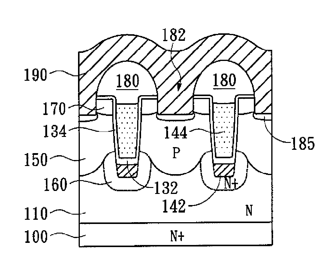
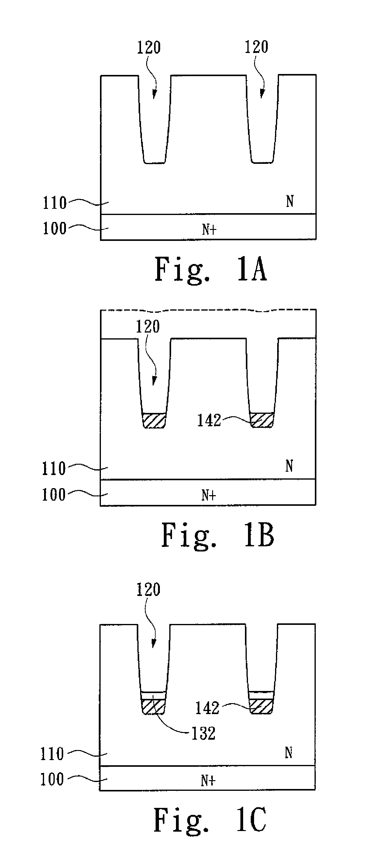
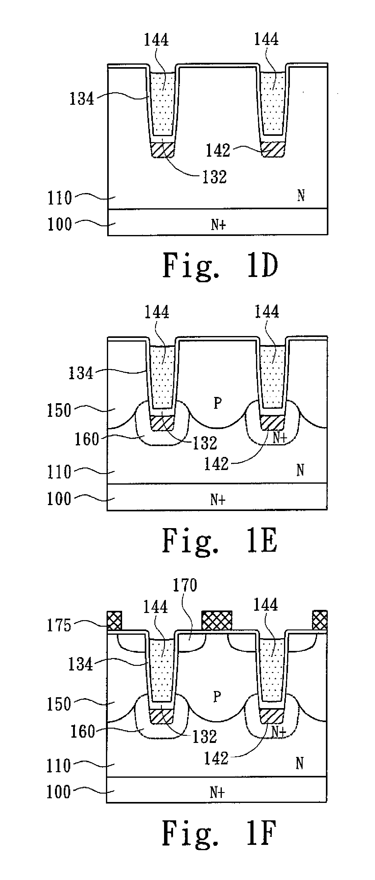
[0016]FIGS. 1A to 1G are schematic views showing a fabrication method of a trenched power semiconductor device in accordance with the present invention. As shown in FIG. 1A, firstly, an N-type substrate 100 is provided, and then an N-type epitaxial layer 110 is formed on the substrate 100 to form a base. Afterward, a trench 120 is formed in the epitaxial layer 110.
[0017]Next, as shown in FIG. 1B, a heavily doped polysilicon layer is deposited over the whole exposed surfaces as shown by the dashed line. Then, the unwanted portion is removed by etching to leave the heavily doped polysilicon structure 142 in the lower portion of the trench 120. Basically, the epitaxial layer 110, which is composed of single crystal material, has an etching speed lower than the polysilicon layer in the same etching environment. With doping concentration being properly adjusted, the etching speed of polysilicon material may reach 10 times the etching speed of epitaxial material. Thus, the polysilicon lay...
second embodiment
[0022]FIG. 2 is a schematic view showing a fabrication method of the trenched power semiconductor device in accordance with the present invention. In the present embodiment, the hard mask 125 is utilized for forming the trenches 120, and the following polysilicon deposition and etching steps are carried out with the hard mask 125 remained on the epitaxial layer 110. The hard mask 125 protects the epitaxial layer 110 therebelow from being etched in the polysilicon etching step.
[0023]FIGS. 3A and 3B are schematic views showing a fabrication method of a trenched power semiconductor device in accordance with a third embodiment of the present invention. In contrast with the first embodiment of the present invention, which features a heavily doped polysilicon structure 142 with a lower surface thereof touching the epitaxial layer 110 as shown in FIG. 1G, the present embodiment has a first dielectric layer 236 formed at the bottom of the trench 120 prior to the formation of the heavily dop...
fourth embodiment
[0024]The above mentioned embodiments describe the technology provided in the present invention being applied to a typical trenched field effect transistor device. But the present invention is not so restricted. As shown in FIGS. 4A to 4C, the present invention describes the technology of the present invention being applied to a high voltage trenched power semiconductor device with the so-called super junction structure.
[0025]As shown in FIG. 4A, firstly, a deep trench 320 is formed in the N-type epitaxial layer 310. Then, as shown in FIG. 4B, a first dielectric layer 3411, a first heavily doped polysilicon layer 3421, a second dielectric layer 3412, a second heavily doped polysilicon layer 3422, and etc., are formed in the deep trench 320 in a serial so as to form a stacked structure with a plurality of dielectric layers 3411,3412, . . . 3416 sandwiched between a plurality of heavily doped polysilicon layers 3421,3422, . . . 3426. The stacked structure with six heavily doped polysi...
PUM
 Abstract
Description
Claims
Application Information