Soi wafer, method for producing same, and method for manufacturing semiconductor device

a technology of silicon dioxide and soi, which is applied in the direction of semiconductor devices, electrical equipment, basic electric elements, etc., can solve the problems that the reduction of device power consumption or the speed-up of devices cannot be achieved effectively, and achieve the effects of good wettability, good wettability and good wettability

Active Publication Date: 2011-12-08
PANASONIC SEMICON SOLUTIONS CO LTD
View PDF5 Cites 76 Cited by
  • Summary
  • Abstract
  • Description
  • Claims
  • Application Information

AI Technical Summary

Benefits of technology

[0041]According to the above structure of the present invention, the gettering layer, which is mainly composed of a silicon which contains one or more of oxygen, carbon and nitrogen and contains at least oxygen, is provided immediately under the monocrystalline silicon layer. When this structure is heated, oxygen is precipitated in the gettering layer and a gettering site is formed. If the gettering layer contains carbon and / or nitrogen as well as oxygen, the carbon and / or nitrogen functions to promote the precipitation of oxygen.
[0042]As explained above, according to the present invention, a gettering site is formed in a layer adjacent to a monocrystalline silicon layer. Thus it exerts a strong gettering ability on the monocrystalline silicon layer.
[0043]On the other hand, the monocrystalline silicon layer, in which semiconductor devices are formed, is a different layer from the gettering layer, and there is no need for the monocrystalline silicon layer to contain oxygen. Thus with the above structure, it is possible to restrict the precipitation of oxygen in the monocrystalline silicon layer, and keep the monocrystalline silicon layer high-quality with little defect.
[0044]Also, according to the present invention, the gettering layer is formed in the SOI wafer in which semiconductor devices have not been formed. Thus the structure eliminates the need to perform a step of forming an impurity diffusion layer in proximity to semiconductor devices as in the “proximity gettering”, in the process of forming the semiconductor devices in the monocrystalline silicon layer. In this respect, the degree of freedom in designing the semiconductor apparatus is ensured.
[0045]Furthermore, according to the manufacturing method of an SOI wafer of the present invention, it is possible to manufacture, at a low cost and with good productivity, the SOI wafer having the above structure of the present invention, namely, the SOI wafer having a strong gettering ability.
[0046]Also, according to the manufacturing method of a semiconductor apparatus of the present invention, it is possible to manufacture a semiconductor apparatus provided with a strong gettering ability by using the above SOI wafer of the present invention. As a result, it is possible to manufacture semiconductor devices having an excellent electric property and reliability.

Problems solved by technology

On the other hand, since such a miniaturization of devices increases the electrostatic capacitance (parasitic capacitance) between wires, and between a silicon substrate and wires, it causes a problem that reduction in power consumption of devices or speed-up of devices cannot be achieved effectively.

Method used


Image

  • Soi wafer, method for producing same, and method for manufacturing semiconductor device
  • Soi wafer, method for producing same, and method for manufacturing semiconductor device
  • Soi wafer, method for producing same, and method for manufacturing semiconductor device

Examples


example 1

of Manufacture of Semiconductor Apparatus

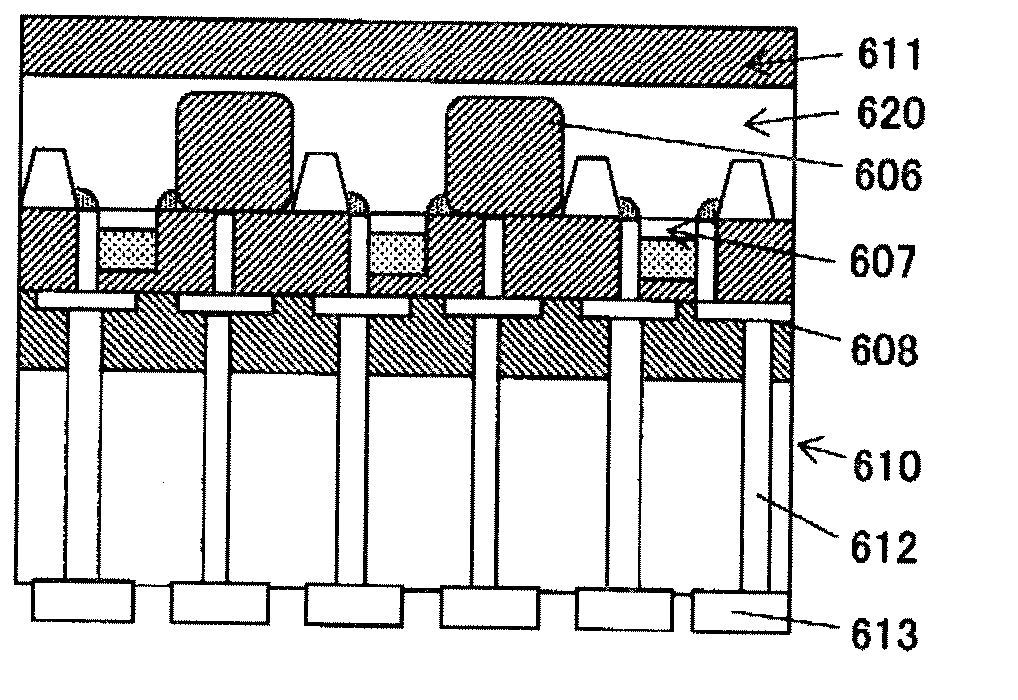
[0173]In this example, a method for manufacturing a backlight imaging device having a photodiode as a buried device will be described.

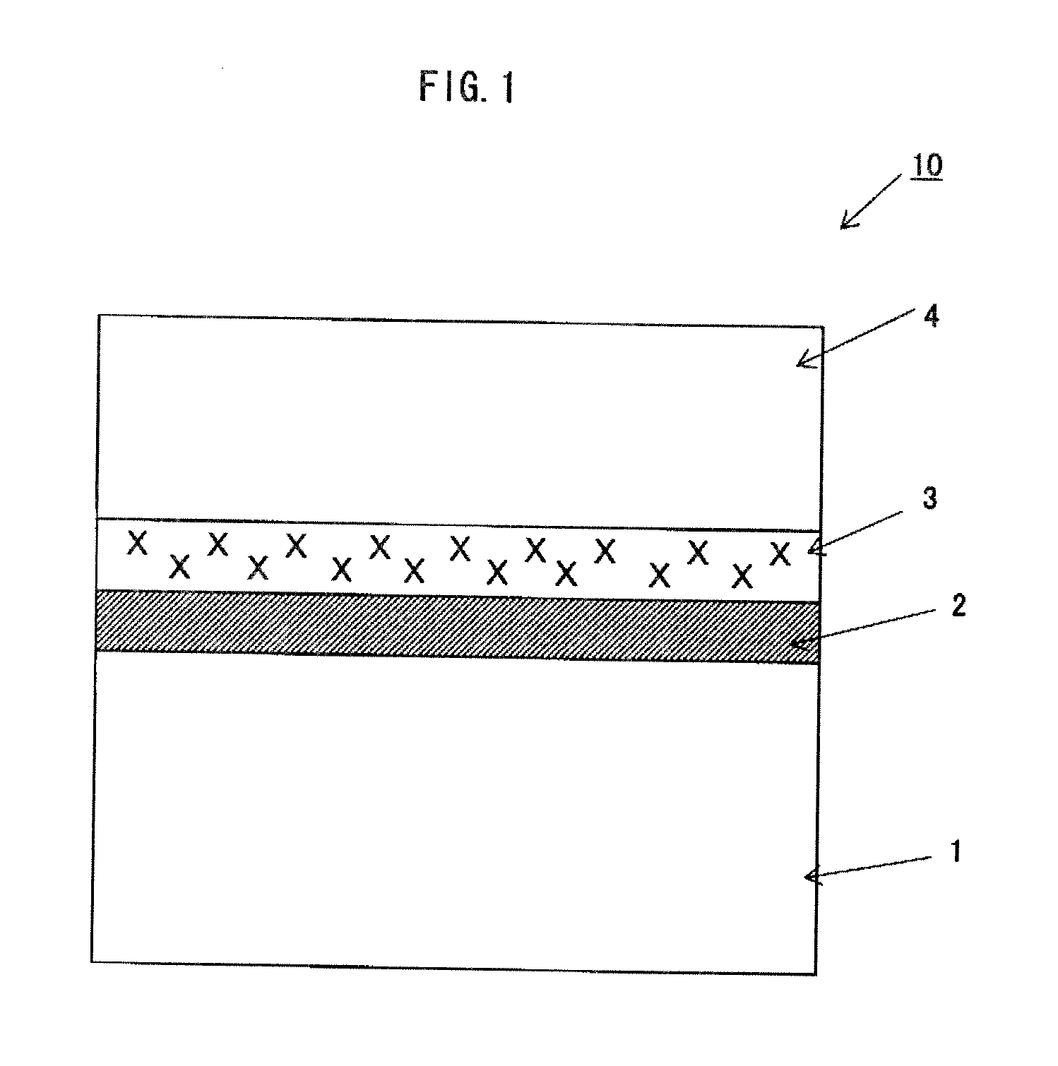
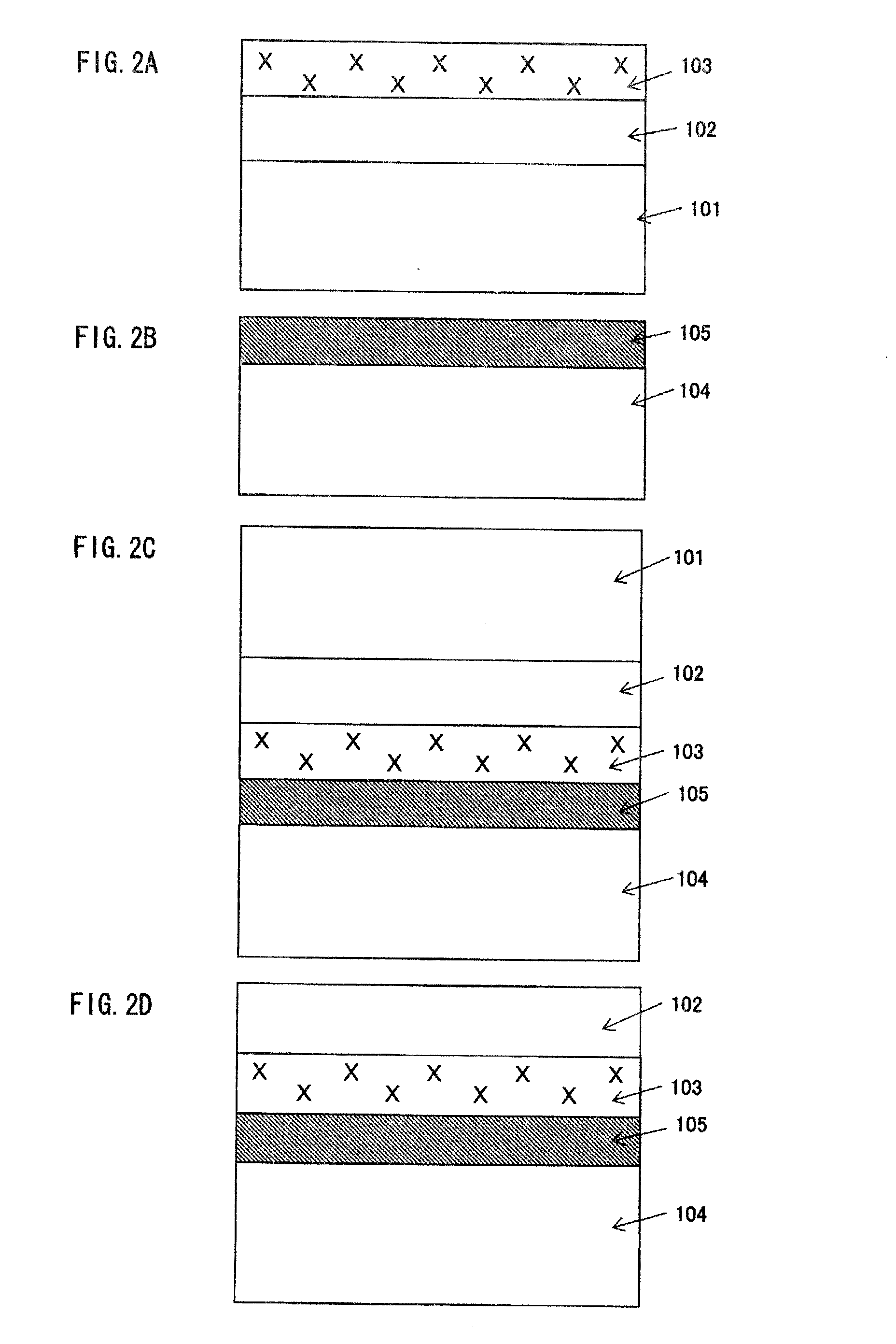
[0174]As shown in FIG. 6A, the SOI wafer as the starting material, includes: a supporting substrate 601 which is a monocrystalline silicon substrate; a BOX layer 602 formed on a surface of the supporting substrate 601; a gettering layer 603 which is mainly composed of a silicon containing oxygen and is formed on a surface of the BOX layer 602; and an S layer 620 which is mainly composed of a P-type monocrystalline silicon and is formed on a surface of the gettering layer 603.

[0175]As the monocrystalline silicon substrate constituting the supporting substrate 601, a P-type, low-resistance substrate having 0.01-0.02 Ωcm of electrical resistivity is used, for which it is taken into account that a heat treatment involving a light irradiation by RTP (Rapid Thermal Processing) or the like needs to be performed in a s...

example 2

of Manufacture of Semiconductor Apparatus

[0196]Next, Example 2 of manufacture of semiconductor apparatus, in which a semiconductor apparatus containing a high-resistance MOS transistor, will be described.

[0197]FIG. 7 illustrates a semiconductor device manufactured by Example 2 of manufacture of semiconductor apparatus. In this Example 2, different from Example 1, the SOI substrate including the gettering layer remains in the semiconductor device as it is.

[0198]An SOI wafer is used as the starting material for forming a semiconductor apparatus, the SOI wafer including: a supporting substrate 701 being a monocrystalline silicon substrate; a BOX layer 702 which is a silicon oxidized layer formed on a surface of the supporting substrate 701; a gettering layer 703 formed on a surface of the BOX layer 702; and an S layer 704 which is mainly composed of a P-type monocrystalline silicon and is formed on a surface of the gettering layer 703.

[0199]In the supporting substrate 701, a P-type, lo...


PUM

PropertyMeasurementUnit
thicknessaaaaaaaaaa
voltageaaaaaaaaaa
thicknessaaaaaaaaaa

Abstract

An SOI wafer including: a supporting substrate 1; a BOX layer 2 provided above the supporting substrate 1, the BOX layer 2 being formed by a thermal oxidization; a gettering layer 3 provided immediately on the BOX layer 2 and mainly composed of a silicon which contains one or more of oxygen, carbon and nitrogen and contains at least oxygen; and an S layer 4 in which semiconductor devices are to be formed, the S layer 4 being mainly composed of a monocrystalline silicon.

Description

[0001]This is a continuation of International Application PCT / JP2010 / 001089, with an international filing date of Feb. 19, 2010.TECHNICAL FIELD[0002]The present invention relates to a structure of a SOI (Silicon-On-Insulator) wafer, a manufacturing method of the SOI wafer, and a manufacturing method of a semiconductor apparatus using the SOI wafer.BACKGROUND ART[0003]In recent years, as semiconductor integrated circuit apparatuses have become highly integrated, highly functional and highly speedy, the devices have been miniaturized more and more. Along with this, not only the horizontal miniaturization as seen in the miniaturization of the gate length of transistors, but the vertical miniaturization as seen in the realization of a very thin gate insulation layer has progressed as well. On the other hand, since such a miniaturization of devices increases the electrostatic capacitance (parasitic capacitance) between wires, and between a silicon substrate and wires, it causes a problem...

Claims


Application Information

Patent Timeline
Patent Type & Authority Applications(United States)
IPC IPC(8): H01L27/12H01L21/762
CPCH01L21/3226H01L21/76243H01L29/78603H01L21/84H01L27/1203H01L21/76254
Inventor YONEDA, KENJI
Owner PANASONIC SEMICON SOLUTIONS CO LTD
Why Eureka
Try Eureka