Photoelectric Conversion Device and Manufacturing Method Thereof

a technology of photoelectric conversion and manufacturing method, which is applied in the direction of semiconductor devices, chemical vapor deposition coatings, coatings, etc., can solve the problems of affecting the character of solar cells and needing attention to contamination, so as to reduce the loss of light due to reflection on the light-receiving surface, prevent contamination of semiconductor substrates, and increase conversion efficiency

Inactive Publication Date: 2011-12-22
SEMICON ENERGY LAB CO LTD
View PDF45 Cites 27 Cited by
  • Summary
  • Abstract
  • Description
  • Claims
  • Application Information

AI Technical Summary

Benefits of technology

[0017]The semiconductor layer which is grown so as to have whiskers as described above functions as an anti-reflection layer. Thus, light loss due to reflection on a light-receiving surface can be reduced and conversion efficiency can be increased.
[0018]Further, when an uneven structure on a light-receiving surface is formed with the use of a special semiconductor coating film which is grown by vapor deposition without etching with an alkaline solution unlike a conventional method, contamination of a semiconductor substrate can be prevented and productivity can be increased.

Problems solved by technology

Etching a photoelectric conversion layer itself in order to form the above uneven structure is not preferable for the following reasons: a problem with controllability for the uneven structure is caused and the characteristics of a solar cell are adversely affected.
Moreover, an alkaline solution and a large amount of rinse water is needed for the etching; thus, attention needs to be paid to contamination.

Method used


Image

  • Photoelectric Conversion Device and Manufacturing Method Thereof
  • Photoelectric Conversion Device and Manufacturing Method Thereof
  • Photoelectric Conversion Device and Manufacturing Method Thereof

Examples


embodiment 1

[0028]In this embodiment, structural examples of a photoelectric conversion device will be described.

[0029]FIGS. 1A to 1C illustrate structural examples of a photoelectric conversion device.

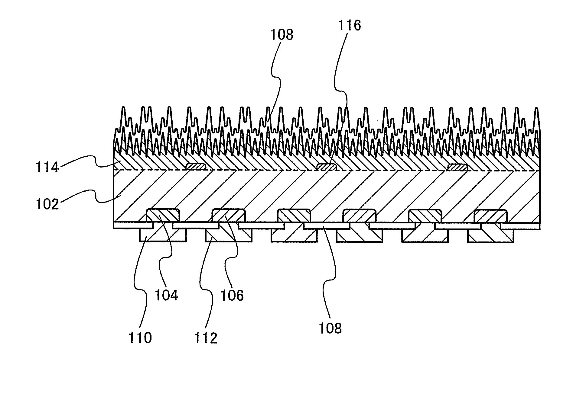
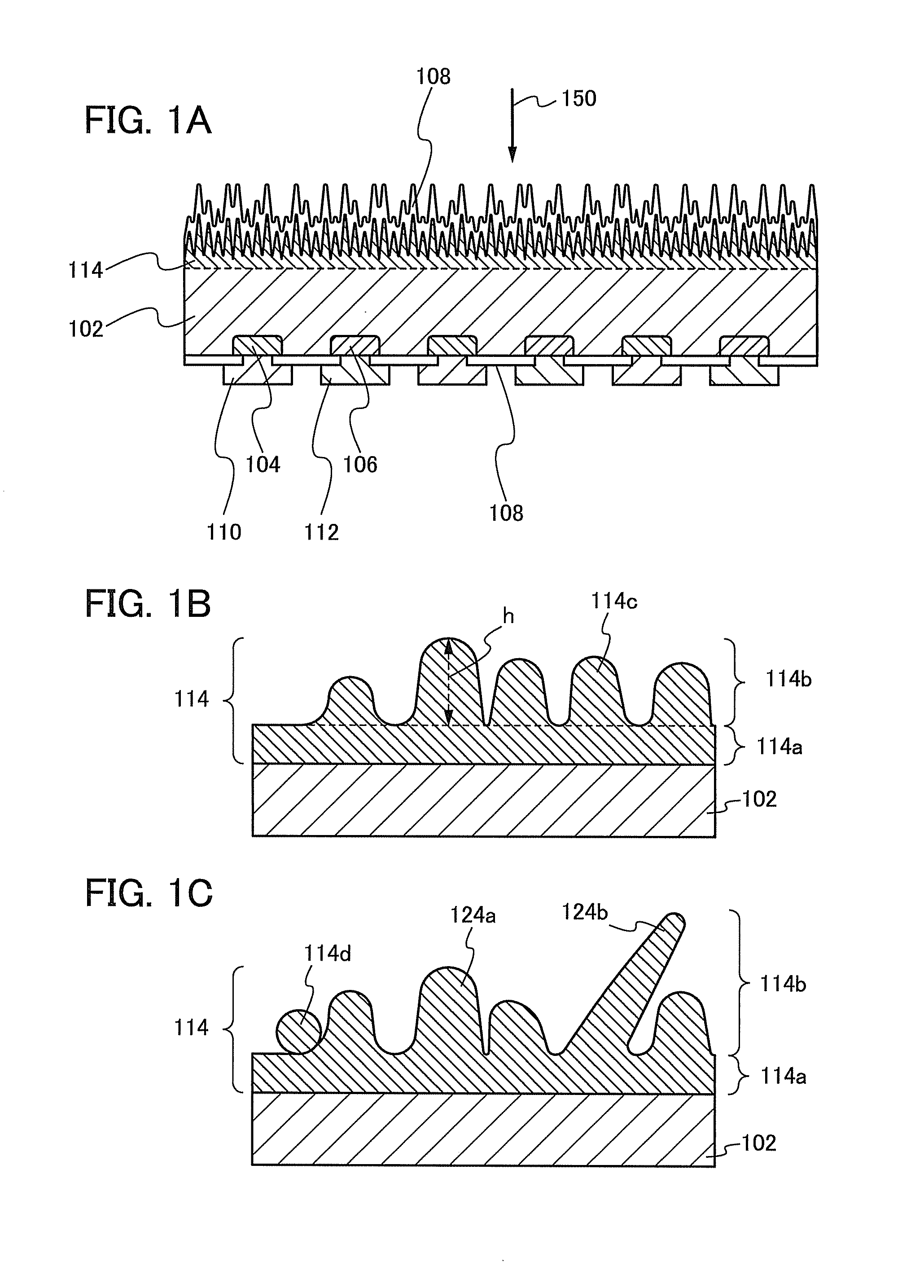
[0030]The photoelectric conversion device includes a semiconductor substrate 102 and receives light from the front surface (also referred to as light-receiving surface) side of the semiconductor substrate 102. In one embodiment of the present invention, the photoelectric conversion device has an uneven structure for reducing reflection of incident light 150 on a front surface of the semiconductor substrate 102. The structure will be specifically described below.

[0031]A group of whiskers 114 is formed on the front surface of the semiconductor substrate 102 as the uneven structure. The group of whiskers 114 can reduce surface reflection of the incident light 150 on the light-receiving surface. The group of whiskers 114 will be specifically described below.

[0032]FIG. 1B is an enlarged view of the gr...

embodiment 2

[0057]In this embodiment, an example of a manufacturing method of a photoelectric conversion device will be described.

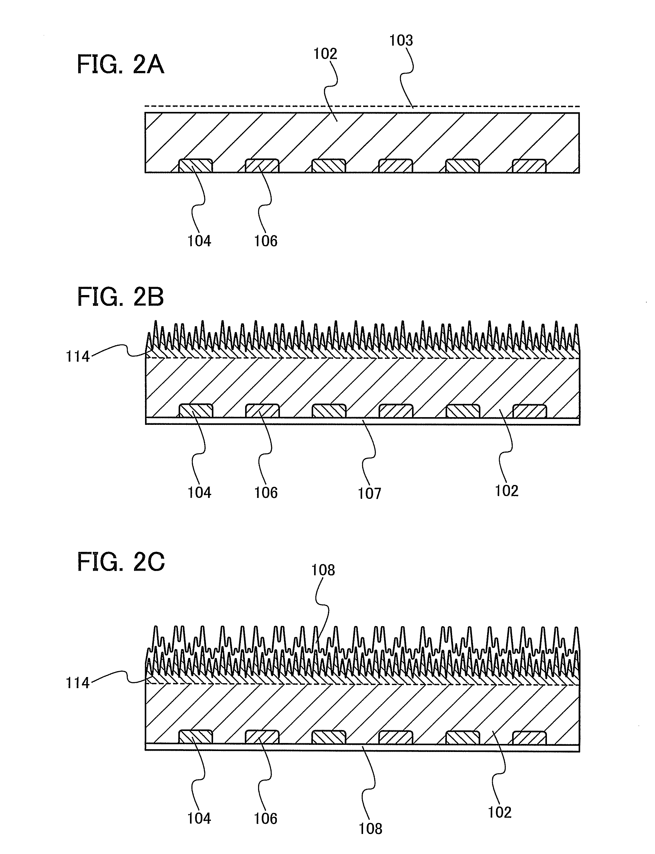
[0058]A metal layer 103 is formed on the front surface (a light-receiving surface) of the semiconductor substrate 102 (FIG. 2A).

[0059]Here, a p-type single crystal silicon substrate is used as the semiconductor substrate 102. Note that an n-type substrate may be used.

[0060]It is preferable that the metal layer 103 be formed to have an extremely small thickness of approximately several nanometers. The extremely small thickness of the metal layer 103 makes it possible to suppress absorption or reflection of incident light from the front surface of the semiconductor substrate 102 by the metal layer 103. Here, the thickness of the metal layer 103 is greater than or equal to 1 nm and less than or equal to 10 nm.

[0061]Further, it is preferable that metal materials contained in the metal layer 103 be dispersed homogeneously in the front surface of the semiconductor substrat...

embodiment 3

[0084]In this embodiment, an example of a manufacturing method of a photoelectric conversion device, which is different from the manufacturing method described in Embodiment 2, will be described.

[0085]In Embodiment 2, the metal layer 103 is formed in a film form on the front surface of the semiconductor substrate 102.

[0086]In contrast, in this embodiment, an island-shaped metal layer is formed on the front surface of the semiconductor substrate 102, instead of the metal layer 103 illustrated in FIG. 2A. The island-shaped metal layer may be formed by a screen printing method, an evaporation method, or the like.

[0087]Accordingly, in a photoelectric conversion device after manufacture, an island-shaped metal layer 116 is provided between the front surface of the semiconductor substrate 102 and the group of whiskers 114 (FIG. 4). When the island-shaped metal layer 116 is formed, reflection or the like can be reduced as compared to the case where a metal layer is formed over the entire s...


PUM

PropertyMeasurementUnit
temperatureaaaaaaaaaa
diameteraaaaaaaaaa
lengthaaaaaaaaaa

Abstract

A photoelectric conversion device with a novel anti-reflection structure. In the photoelectric conversion device, a front surface of a semiconductor substrate which serves as a light-receiving surface is covered with a group of whiskers (a group of nanowires) so that surface reflection is reduced. In other words, a semiconductor layer which has a front surface where crystals grow so that whiskers are formed is provided on the light-receiving surface side of the semiconductor substrate. The semiconductor layer has a given uneven structure, and thus has effects of reducing reflection on the front surface of the semiconductor substrate and increasing conversion efficiency.

Description

BACKGROUND OF THE INVENTION[0001]1. Field of the Invention[0002]The present invention relates to a photoelectric conversion device. One embodiment of the disclosed invention includes a back contact element structure.[0003]2. Description of the Related Art[0004]A solar cell in which a single crystal silicon substrate or a polycrystalline silicon substrate is used for a photoelectric conversion layer has been developed as one of photoelectric conversion devices. In such a solar cell, an uneven structure is formed on a front surface of the silicon substrate in order to reduce surface reflection. This uneven structure is formed by etching the silicon substrate with an alkaline solution such as NaOH. An alkaline solution has different etching rates depending on crystal plane orientations of silicon. Thus, for example, when a silicon substrate which has a crystal plane orientation of (100) is etched, a pyramidal uneven structure is formed. Back contact solar cells which have such an uneve...

Claims


Application Information

Patent Timeline
Patent Type & Authority Applications(United States)
IPC IPC(8): H01L31/0232H01L31/0236H01L31/06H01L31/18C01B33/02C23C16/24H01L31/0216H01L31/04H01L31/068
CPCH01L31/02168H01L31/02363H01L31/022441Y02E10/547H01L31/0682C01B33/02C23C16/24H01L31/0232H01L31/0236H01L31/04H01L31/06H01L31/18
Inventor YAMAZAKI, SHUNPEIARAI, YASUYUKI
Owner SEMICON ENERGY LAB CO LTD
Why Eureka
Try Eureka