Rectification element and method for resistive switching for non volatile memory device

a resistive switching and memory device technology, applied in the direction of emergency protective circuit arrangement, emergency protective arrangement for limiting excess voltage/current, instruments, etc., can solve the problems of increasing power dissipation, preventing proper device operation, and non-scaling of sub-threshold slopes, so as to improve leakage current characteristics, high switching speed, and high density. non-volatile

Active Publication Date: 2011-12-29
RGT UNIV OF MICHIGAN
View PDF14 Cites 132 Cited by
  • Summary
  • Abstract
  • Description
  • Claims
  • Application Information

AI Technical Summary

Benefits of technology

[0011]Many benefits are achieved by ways of the present invention over conventional techniques. For example embodiments of the present invention allow for a high density non-volatile device characterized by high switching speed, improved leakage current characteristic, and high device yield. Depending on the embodiment, one or more of these benefits may be achieved. These and other benefits will be described in more detail throughout the present specification and more particularly below.

Problems solved by technology

However, as field effect transistors (FET) approach sizes less than 100 nm, problems such as short channel effect start to prevent proper device operation.
Moreover, such sub 100 nm device size can lead to sub-threshold slope non-scaling and also increases power dissipation.
These devices often require new materials and device structures to couple with silicon based devices to form a memory cell, which lack one or more key attributes.
For example, Fe-RAM and MRAM devices have fast switching characteristics and good programming endurance, but their fabrication is not CMOS compatible and size is usually large.
Switching for a PCRAM device uses Joules heating, which inherently has high power consumption.
Organic RAM or ORAM is incompatible with large volume silicon based fabrication and device reliability is usually poor.

Method used


Image

  • Rectification element and method for resistive switching for non volatile memory device
  • Rectification element and method for resistive switching for non volatile memory device
  • Rectification element and method for resistive switching for non volatile memory device

Examples


Embodiment Construction

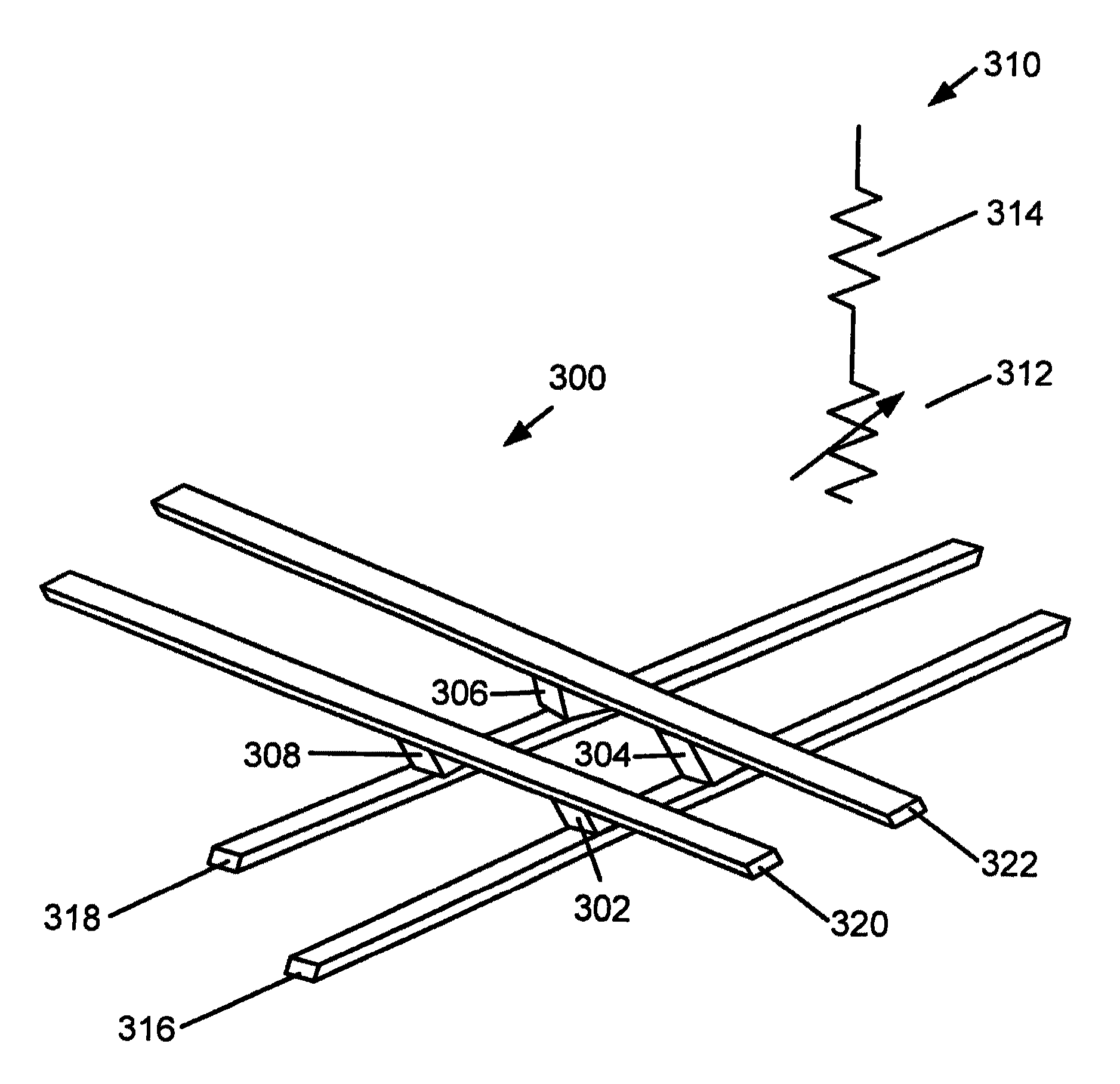
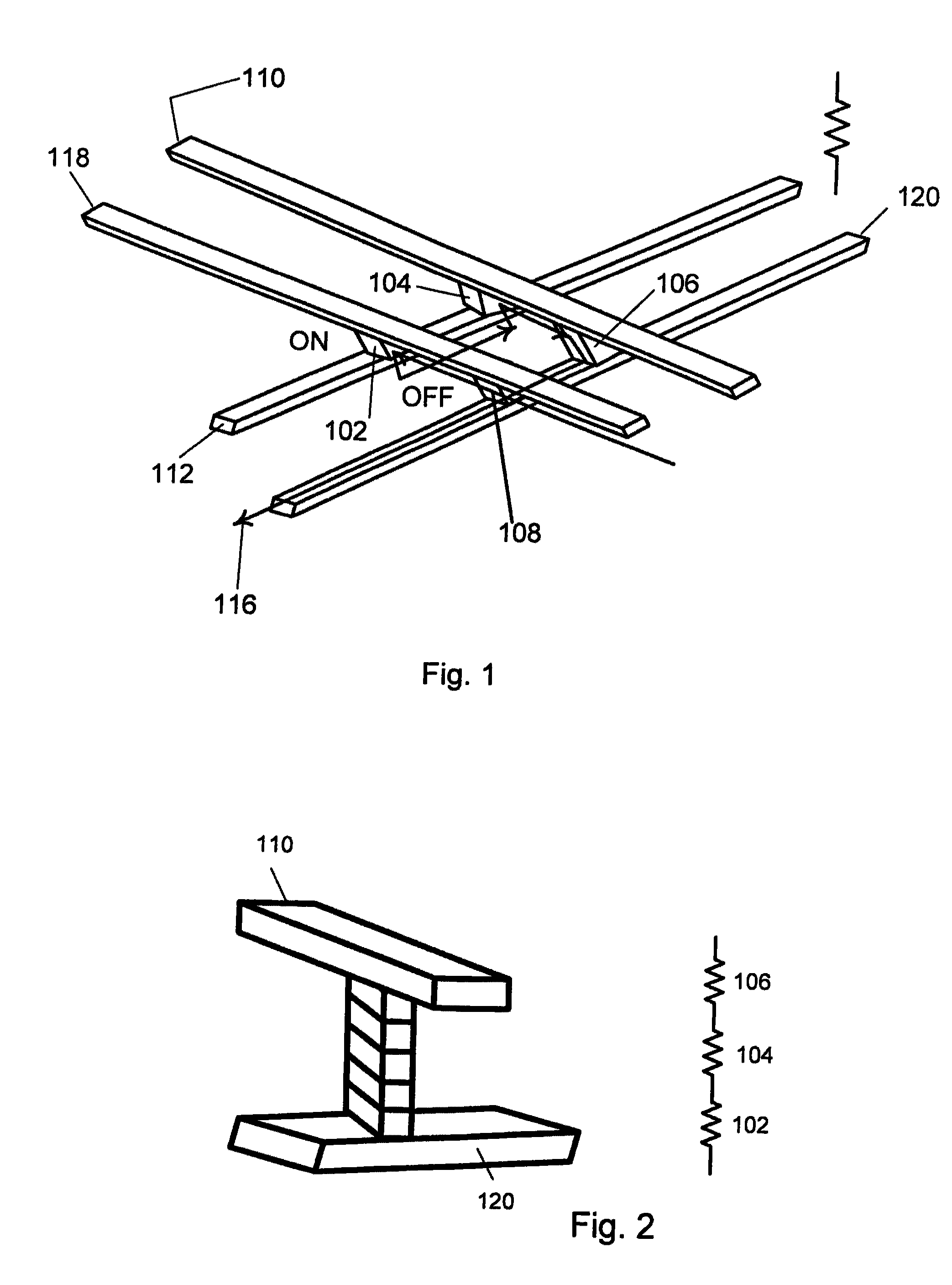
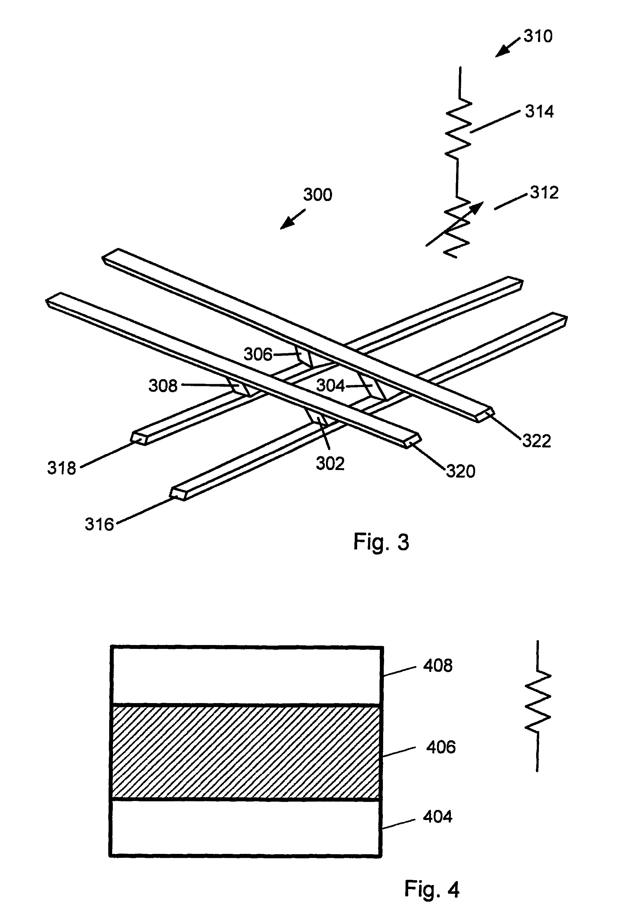
[0019]The illustrated embodiment described below is generally directed to a memory device that uses a resistive switching device having integrated rectification functionality. The switching device may be used in a RRAM or ReRAM or any highly interconnected and highly integrated devices. But it should be recognized that embodiments of the present invention can have a broader range of applicability.

[0020]RRAM can be a two terminal device in which a switching element is sandwiched between a top electrode and a bottom electrode. The resistance of the switching element is varied by applying a voltage to the electrodes or a current through the switching element. Resistive switching can be bipolar or unipolar. In bipolar switching, the change in resistance of the switching element depends on polarity and a magnitude of an applied voltage or an applied current. In the case of unipolar switching, the change in resistance of the switching element depends only on the magnitude of the applied v...


PUM

PropertyMeasurementUnit
thicknessaaaaaaaaaa
dielectric constantaaaaaaaaaa
sizesaaaaaaaaaa

Abstract

A method of suppressing propagation of leakage current in an array of switching devices. The method includes providing a dielectric breakdown element integrally and serially connected to a switching element within each of the switching device. A read voltage (for example) is applied to a selected cell. The propagation of leakage current is suppressed by each of the dielectric breakdown element in unselected cells in the array. The read voltage is sufficient to cause breakdown in the selected cells but insufficient to cause breakdown in the serially connected, unselected cells in a specific embodiment. Methods to fabricate of such devices and to program, to erase and to read the device are provided.

Description

CROSS-REFERENCE TO RELATED APPLICATION[0001]This application claims the priority of U.S. Provisional Patent Application No. 61 / 358,378, filed Jun. 24, 2010, the entire contents of which are hereby incorporated by reference.STATEMENT RELATED TO FEDERAL FUNDING[0002]This invention was made with government support under CCF0621823 awarded by the National Science Foundation. The government has certain rights in the invention.COPYRIGHT NOTICE[0003]A portion of the disclosure of this patent document contains material that is subject to copyright protection. The copyright owner has no objection to the facsimile reproduction by anyone of the patent document or the patent disclosure as it appears in the Patent and Trademark Office patent file or records, but otherwise reserves all copyright rights whatsoever.BACKGROUND[0004]The present invention is related to switching devices. More particularly, the present invention provides a structure and a method that can be used for forming a non-volat...

Claims


Application Information

Patent Timeline
Patent Type & Authority Applications(United States)
IPC IPC(8): G11C11/00H01L45/00H02H3/00
CPCG11C13/0007H01L45/148G11C13/004G11C13/0069G11C13/0097G11C2213/33G11C2213/76H01L27/2409H01L27/2463H01L45/04H01L45/08H01L45/085H01L45/1233H01L45/141H01L45/146H02H9/08H01L45/12G11C13/003H10B63/80H10N70/24H10N70/801H10N70/245H10N70/826H10N70/884H10N70/8833H10B63/20H10N70/023H10N70/20H10N70/881H10N70/882
Inventor LU, WEIJO, SUNG HYUN
Owner RGT UNIV OF MICHIGAN
Why Eureka
Try Eureka