
Metal-Coated Polyimide Resin Substrate with Excellent Thermal Aging Resistance Properties

a technology of metal-coated polyimide resin and thermal aging resistance, which is applied in the direction of superimposed coating process, liquid/solution decomposition chemical coating, synthetic resin layered products, etc., can solve problems such as differences, and achieve the effect of increasing adhesion and superior effects in formation

Inactive Publication Date: 2011-12-29
JX NIPPON MINING& METALS CORP
View PDF3 Cites 5 Cited by
  • Summary
  • Abstract
  • Description
  • Claims
  • Application Information

AI Technical Summary

Benefits of technology

[0019]The metal-coated polyimide resin substrate of the present invention yields superior effects in the formation of fine patterns as a result of being able to increase the adhesion after aging without deteriorating the initial adhesion between the polyimide film and the metal layer after lamination.

Problems solved by technology

Even if the thickness of the modification layer is the same in the foregoing evaluation, there was a problem in that differences would arise with the actual results of peel strength test.Patent Document 1: Japanese Patent No. 3173511Patent Document 2: Published Japanese Translation No. 2003-519901 of PCT ApplicationPatent Document 3: Japanese Laid-Open Patent Publication No. 2005-154895Patent Document 4: Japanese Laid-Open Patent Publication No. 2007-318177

Method used


Image

  • Metal-Coated Polyimide Resin Substrate with Excellent Thermal Aging Resistance Properties
  • Metal-Coated Polyimide Resin Substrate with Excellent Thermal Aging Resistance Properties

Examples


example 1

[0037]As the polyimide resin film, Kapton 150EN manufactured by Du Pont was used. The polyimide resin film was immersed in a potassium hydroxide solution as the surface modification process, and washed with deionized water. Subsequently, as the catalyst-adding step, the foregoing polyimide resin film was immersed in a solution in which a silane coupling agent containing a functional group with metal binding capability was mixed or reacted with a noble metal compound, and washed with deionized water.

[0038]After the foregoing treatment, as the electroless plating step, an electroless nickel-boron-based plating solution was used to form a nickel layer of 0.15 μm, this was washed with deionized water, heat treatment was thereafter performed at 150° C. to form a nickel layer of 0.05 μm, this was washed with deionized water, and a nickel layer in a total amount of 0.20 μm was formed. Subsequently, an electroless copper seed layer was formed on the nickel layer with an electroless copper p...

example 2

[0043]As the polyimide resin film, Kapton 150EN manufactured by Du Pont was used. The polyimide resin film was subject to UV irradiation and thereafter immersed in sulfuric acid as the surface modification process, and this was subsequently washed with deionized water. Subsequently, as the catalyst-adding step, the foregoing polyimide resin film was immersed in a solution in which a silane coupling agent containing a functional group with metal binding capability was mixed or reacted with a noble metal compound, and washed with deionized water.

[0044]After the foregoing treatment, as the electroless plating step, an electroless nickel-boron-based plating solution was used to form a nickel layer of 0.2 μm, this was washed with deionized water. Subsequently, an electroless copper seed layer was formed on the nickel layer with an electroless copper plating solution, and a copper conductor layer of 8 μm was thereafter formed by electroplating.

[0045]The strength on 90-degree peeling was m...

example 3

[0049]As the polyimide resin film, Kapton 150EN manufactured by Du Pont was used. The polyimide resin film was subject to UV irradiation and thereafter immersed in nitric acid as the surface modification process, and this was subsequently washed with deionized water. Subsequently, as the catalyst-adding step, the foregoing polyimide resin film was immersed in a solution in which a silane coupling agent containing a functional group with metal binding capability was mixed or reacted with a noble metal compound, and washed with deionized water.

[0050]After the foregoing treatment, as the electroless plating step, an electroless nickel-boron-based plating solution was used to form a nickel layer of 0.15 μm, this was washed with deionized water, heat treatment was thereafter performed at 150° C. to form a nickel layer of 0.05 μm, this was washed with deionized water, and a nickel layer in a total amount of 0.20 μm was formed. Subsequently, an electroless copper seed layer was formed on t...


PUM

PropertyMeasurementUnit
Temperatureaaaaaaaaaa
Fractionaaaaaaaaaa
Fractionaaaaaaaaaa

Abstract

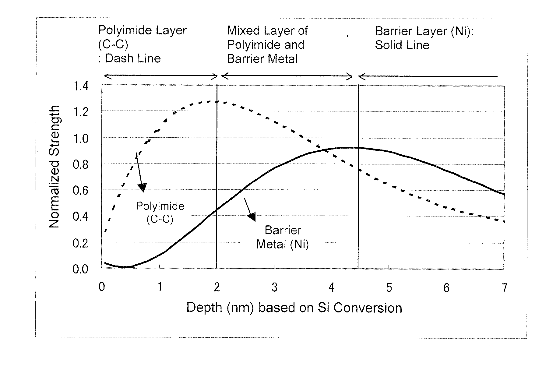
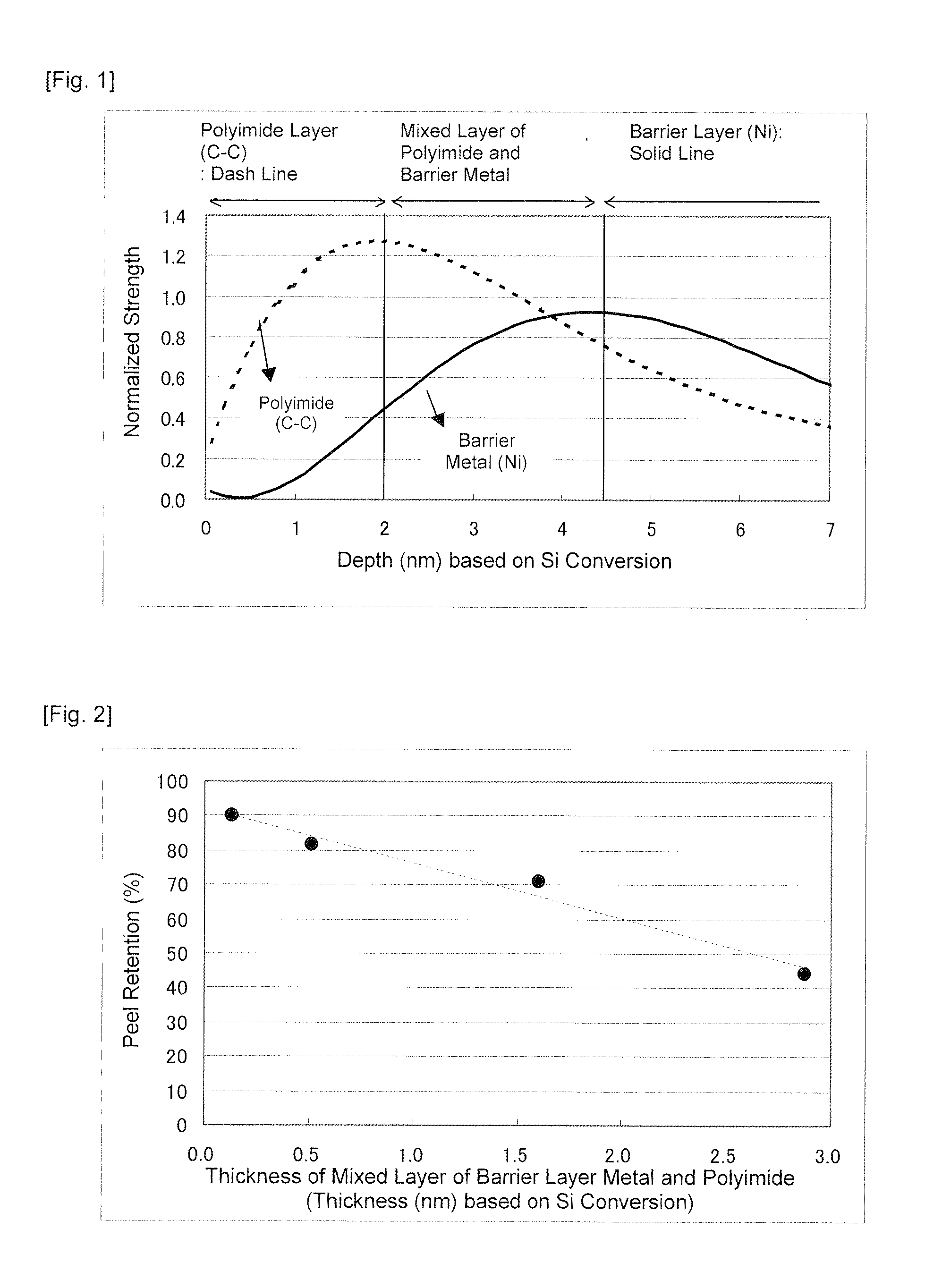
[Object] To provide a metal-coated polyimide resin substrate that does not deteriorate the initial adhesion between the metal-coated polyimide resin film and the metal layer and has high adhesion after aging at 150° C. for 168 hours.[Solution] A metal-coated polyimide resin substrate in which a barrier layer is formed by a wet process after performing surface modification to one surface or both surfaces of a polyimide resin film by a wet process or a dry process or a combination thereof, a seed layer is thereafter formed by a wet process or a dry process, and a conductive film is formed on a surface layer thereof by a wet process; wherein, at the peeling surface on the conductive film layer side after the metal-coated polyimide resin substrate is subject to a 90-degree peel test, the thickness of a mixed layer of polyimide residue and barrier metal layer residue according to in-depth profiling with a time-of-flight secondary ion mass spectrometer (TOF-SIMS) is 2.60 nm or less based on Si sputter rate conversion, and peel strength retention after an aging test at 150° C. for 168 hours (peel strength after aging at 150° C. for 168 hours / initial peel strength) is 50% or higher.

Description

TECHNICAL FIELD[0001]The present invention relates to an adhesive-free flexible laminate material for use as a mounting material of electronic components such as a flexible print substrate, TAB and COF, and in particular relates to a metal-coated polyimide resin substrate with excellent thermal aging resistance properties.BACKGROUND ART[0002]An FCCL (Flexible Copper Clad Laminate), in which metal conductor layers primarily formed from copper are laminated on a polyimide film, is broadly used as a circuit board material in the electronics industry. Among the above, an adhesive-free flexible laminate (particularly a two-layer flexible laminate) that does not comprise an adhesive layer between a polyimide film and a metal layer is attracting attention pursuant to the demands of finer pitches of the circuit wiring width.[0003]As a method of producing an adhesive-free flexible laminate, in particular an adhesive-free flexible laminate capable of accommodating fine pitches; there is a so-...

Claims


Application Information

Patent Timeline
IPC IPC(8): B32B27/06B32B33/00
CPCC23C18/1651C23C18/2006C23C18/204C23C18/24C25D5/56H05K1/0346Y10T428/12535H05K3/381H05K3/388H05K2201/0154H05K2201/0344H05K2201/2063H05K3/181Y10T428/31721B32B15/088C23C18/20C23C28/02H05K3/24
Inventor YOSHIDA, TAKU
Owner JX NIPPON MINING& METALS CORP
Learn More