Large Area Nitride Crystal and Method for Making It

Inactive Publication Date: 2012-01-05
SORAA
View PDF4 Cites 133 Cited by
  • Summary
  • Abstract
  • Description
  • Claims
  • Application Information

AI Technical Summary

Benefits of technology

[0008]This invention provides a method for growth of a large-area, gallium-containing nitride crystal. The method includes providing at least two nitride crystals having a dislocation density below about 107 cm−2 together with a handle substrate. The nitride crystals are bonded to the handle substrate. Then the nitride crystals are grown to coalescence into a merged nitride crystal. The polar misorientation angle γ between the first nitride crystal and the second nitride crystal is less than 0.5 degree and azimuthal misorientation angles α and β are less than 1 degree. A semiconductor structure can be formed on the nitride crystals as desired.
[0009]In another embodiment, the invention includes the steps above, but also includes providing a release layer and a high quality epitaxial layer on each o

Problems solved by technology

The typical average dislocation density, however, in these crystals, about 106-108 cm−2, is undesirably high for many applications.
Techniques have been developed to gather the dislocations into bundles or low-angle grain boundaries, but it is still very difficult to produce dislocation densities below 104 cm−2 in a large area single grain by these methods, and the relatively high concentration of high-dislocation-density bundles or grain boundaries creates difficulties, performance degradation, and/or yield losses for the device manufacturer.
Unfortunately, no large area, high quality non-polar or semi-polar GaN wafers are generally available for large scale commercial applications.
These cr

Method used


Image

  • Large Area Nitride Crystal and Method for Making It
  • Large Area Nitride Crystal and Method for Making It
  • Large Area Nitride Crystal and Method for Making It

Examples


Example

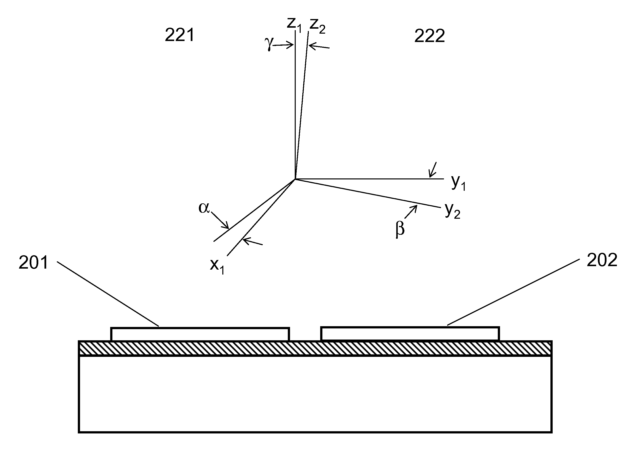
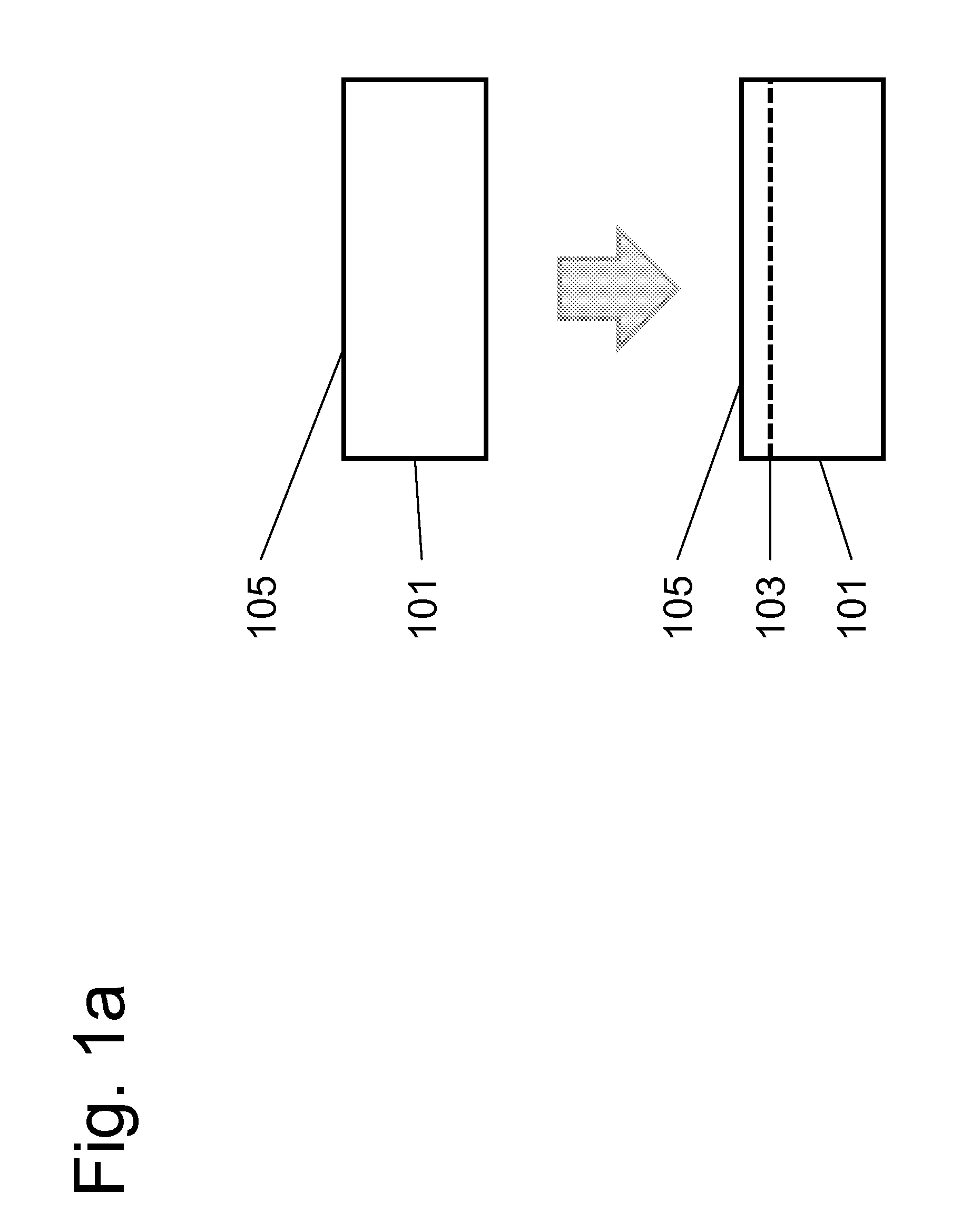
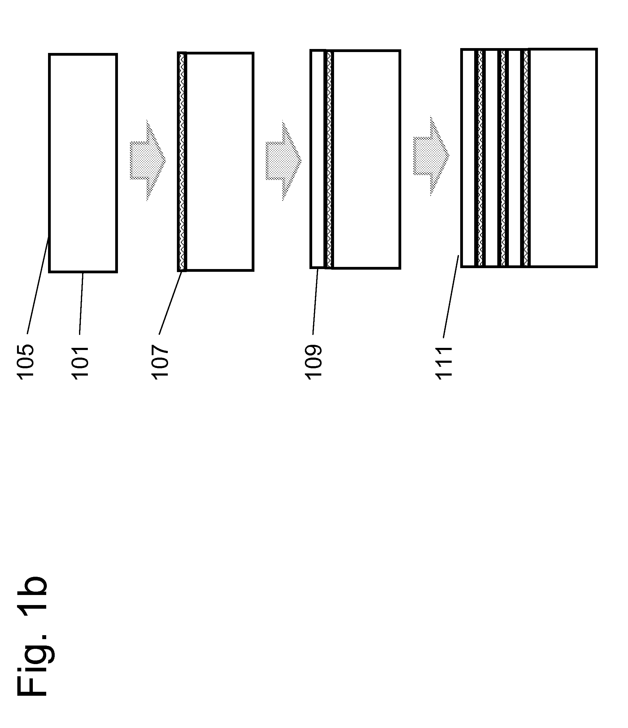
[0017]Referring to FIG. 1a, a crystal 101 having a first surface 105 is provided. We will often refer to crystal 101 as a “nitride crystal”, as nitride crystals with a wurtzite crystal structure comprise a preferred embodiment. The method disclosed, however, has broader generality, and the term “nitride crystal” should be understood to include non-nitride crystals as well as nitride crystals. Examples of non-nitride crystals for which this invention may be applicable include diamond, cubic boron nitride, boron carbide, silicon, germanium, silicon germanium, indium phosphide, gallium phosphide, zinc oxide, zinc selenide, gallium arsenide, cadmium telluride, and cadmium zinc telluride. In preferred embodiments, nitride crystal 101 comprises GaN or AlxInyGa(1−x−y)N, where 0≦x, y≦1 and has a very high crystallographic quality. In another embodiment, crystal 101 has a wurtzite crystal structure and is ZnO, ZnS, AgI, CdS, CdSe, 2H-SiC, 4H-SiC, and 6H-SiC. Nitride crystal 101 preferably ha...


PUM


Abstract

Techniques for processing materials in supercritical fluids include processing in a capsule disposed within a high-pressure apparatus enclosure. The invention is useful for growing crystals of: GaN; AN; InN; and their alloys, namely: InGaN; AlGaN; and AlInGaN; for manufacture of bulk or patterned substrates, which in turn can be used to make optoelectronic devices, lasers, light emitting diodes, solar cells, photoelectrochemical water splitting and hydrogen generation, photodetectors, integrated circuits, and transistors.

Description

CROSS REFERENCE TO RELATED APPLICATIONS[0001]This application claims priority to U.S. Provisional Application No. 61 / 356,489, filed Jun. 18, 2010; and U.S. Provisional Application No. 61 / 386,879, filed Sep. 27, 2010, each of which is incorporated herein by reference for all purposes.BACKGROUND OF THE INVENTION[0002]This invention relates to techniques for processing materials in supercritical fluids. Embodiments of the invention include techniques for material processing in a capsule disposed within a high-pressure apparatus enclosure. The invention can be applied to growing crystals of: GaN; AN; InN; and their alloys, namely: InGaN; AlGaN; and AlInGaN; and others for manufacture of bulk or patterned substrates. Such bulk or patterned substrates can be used for a variety of applications including optoelectronic devices, lasers, light emitting diodes, solar cells, photoelectrochemical water splitting and hydrogen generation, photodetectors, integrated circuits, and transistors, among...

Claims


Application Information

Patent Timeline
IPC IPC(8): C30B25/02C30B23/02
CPCC30B25/02C30B33/06C30B29/403C30B25/18H01L21/185
Inventor D'EVELYN, MARK P.SPECK, JAMES S.
Owner SORAA
Why Eureka
Try Eureka