Semiconductor Device and Manufacturing Method Thereof

a semiconductor and semiconductor technology, applied in semiconductor devices, semiconductor/solid-state device details, electrical devices, etc., can solve the problems of difficult formation of diffusion prevention films uniformly on side surfaces and bottom surfaces of grooves and contact holes, and achieve favorable electric characteristics and high yield

Inactive Publication Date: 2012-01-05
SEMICON ENERGY LAB CO LTD
View PDF12 Cites 4 Cited by
  • Summary
  • Abstract
  • Description
  • Claims
  • Application Information

AI Technical Summary

Benefits of technology

[0008]As a thin film transistor is further miniaturized to improve productivity and to save size of a semiconductor device, it becomes difficult to form a diffusion prevention film uniformly on side surfaces and a bottom surface of a groove and a contact hole.
[0010]A sputtering method is widely used to form a conductive film for the reasons as follows: deposition rate is high; an apparatus has a relatively simple structure and is inexpensive; and a large area can also be processed by a sputtering method. When a film is formed by a sputtering method, the film has such a problem that a groove and a contact hole have an overhang shape and that the film is not deposited uniformly on the side surfaces and the bottom surface of the groove and the contact hole. When a portion where coverage with a diffusion prevention film is insufficient is generated, diffusion of the wiring material with a low resistance into the semiconductor film is caused, leading to an increase in off-state current of a thin film transistor.
[0011]On the other hand, a fine groove and a fine contact hole in a film formed by an ALD method do not have an overhang shape, and the film can be deposited uniformly on the side surface and the bottom surface of the groove and the contact hole. However, as compared to a sputtering method, an apparatus used in an ALD method is expensive, a large area is hard to be processed by an ALD method, and deposition rate of an ALD method is low.
[0013]Another object of one embodiment of the present invention is to provide a method for manufacturing a semiconductor device which has excellent electric characteristics with a high yield.
[0030]According to one embodiment of the present invention, a diffusion prevention film can be uniformly formed on the side surfaces and the bottom surface of a groove and a contact hole; thus, even when a wiring material with a low resistance is used, an increase of off-state current due to diffusion of the wiring material with a low resistance into a semiconductor film or to the periphery of the semiconductor film can be suppressed. Accordingly, a semiconductor device having favorable electric characteristics can be manufactured with a high yield.

Problems solved by technology

When the wiring material with a low resistance is used, diffusion of the wiring material with a low resistance into a semiconductor film becomes a problem.
As a thin film transistor is further miniaturized to improve productivity and to save size of a semiconductor device, it becomes difficult to form a diffusion prevention film uniformly on side surfaces and a bottom surface of a groove and a contact hole.
When a film is formed by a sputtering method, the film has such a problem that a groove and a contact hole have an overhang shape and that the film is not deposited uniformly on the side surfaces and the bottom surface of the groove and the contact hole.
When a portion where coverage with a diffusion prevention film is insufficient is generated, diffusion of the wiring material with a low resistance into the semiconductor film is caused, leading to an increase in off-state current of a thin film transistor.

Method used


Image

  • Semiconductor Device and Manufacturing Method Thereof
  • Semiconductor Device and Manufacturing Method Thereof
  • Semiconductor Device and Manufacturing Method Thereof

Examples


embodiment 1

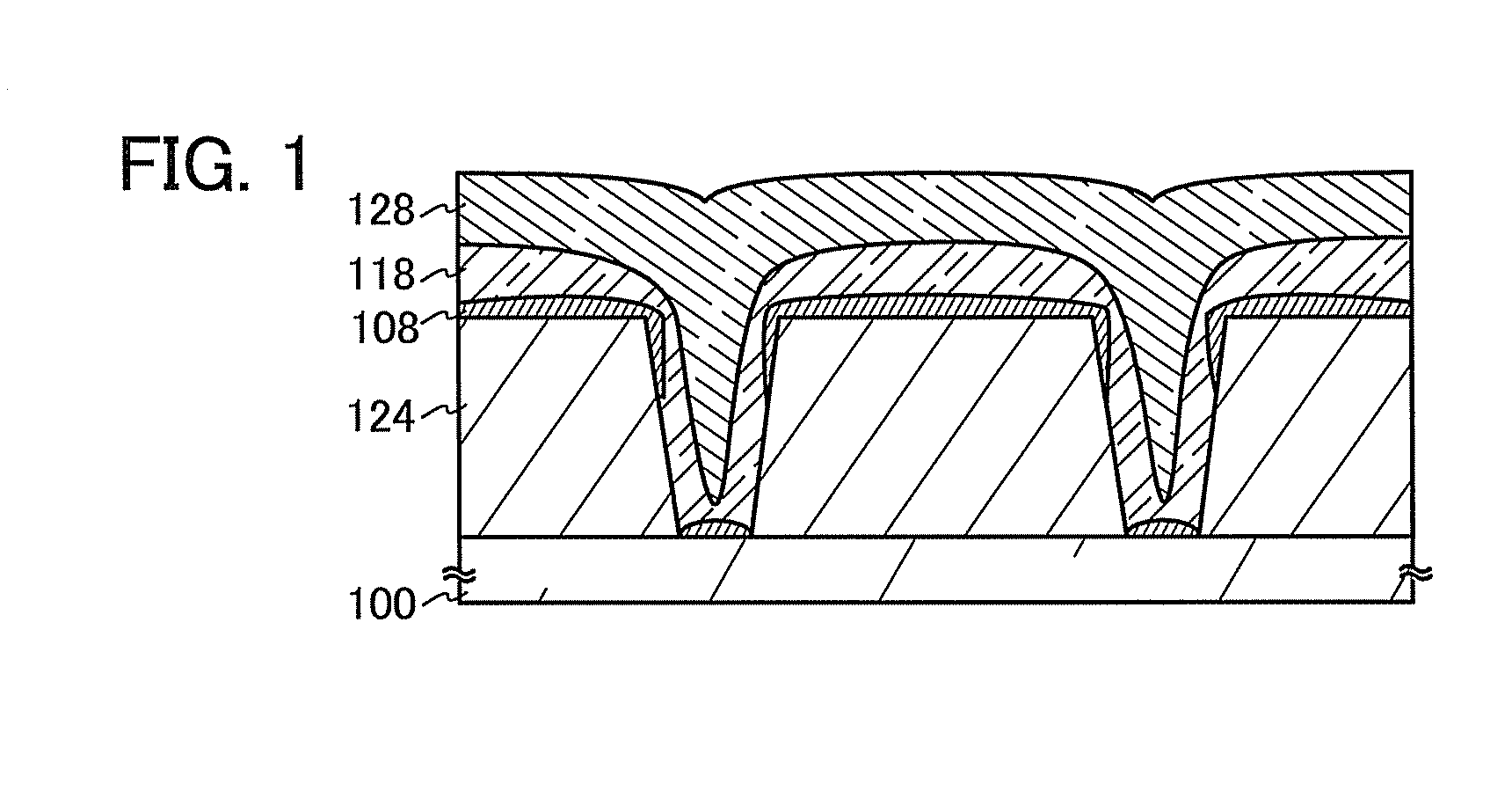
[0039]In this embodiment, a cross-sectional structure of a semiconductor device according to one embodiment of the present invention will be described with reference to FIG. 1.

[0040]FIG. 1 shows a cross-sectional view of a semiconductor device including a substrate 100, an insulating film 124, a groove or a contact hole formed in the insulating film 124, a conductive film 118, and a conductive film 128. A conductive film 108 may be formed between the insulating film 124 and the conductive film 118 and / or between the substrate 100 and the conductive film 118.

[0041]As the substrate 100, a glass substrate, a ceramic substrate, or a plastic substrate over which a semiconductor region or a conductive region is provided can be used. Alternatively, a silicon wafer, an SOI (silicon on insulator) substrate, a semiconductor substrate such as a gallium arsenide substrate can be used. Further alternatively, a metal substrate of a stainless alloy or the like can be used. As the glass substrate, ...

embodiment 2

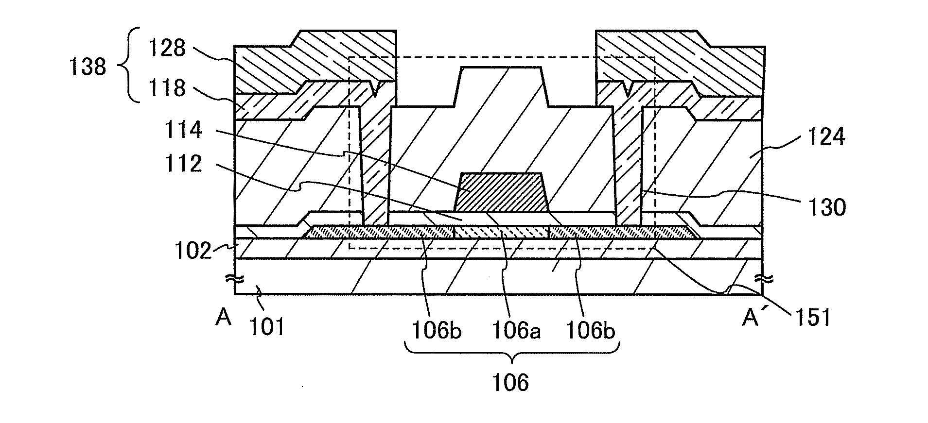
[0073]In this embodiment, a planar structure and a cross-sectional structure of a thin film transistor 151 which can be used in a semiconductor device according to one embodiment of the present invention will be described with reference to FIGS. 3A and 3B. FIG. 3A is a plane view and FIG. 3B is a cross-sectional view taken along line A-A′ in FIG. 3A. Note that in FIG. 3A, some of components of the thin film transistor 151 (for example, a gate insulating film 112) are omitted for brevity.

[0074]The thin film transistor 151 shown in FIGS. 3A and 3B includes a substrate 101, a base insulating film 102 over the substrate 101, a semiconductor film 106 over the base insulating film 102, the gate insulating film 112 covering the semiconductor film 106, a gate electrode 114 over the semiconductor film 106 provided with the gate insulating film 112 therebetween, an insulating film 124 covering the gate insulating film 112 and the gate electrode 114, a contact hole 130 formed in the insulating...

embodiment 3

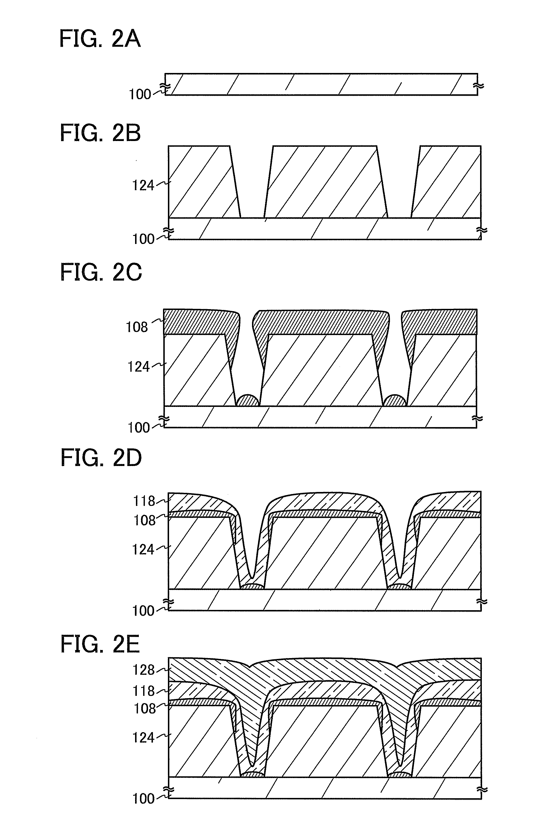
[0085]A method for manufacturing the thin film transistor 151 described in Embodiment 2 will be described with reference to FIGS. 4A to 4E and FIGS. 5A to 5C.

[0086]First, the substrate 101 is prepared.

[0087]In the case where a thin film transistor is provided over a flexible substrate as the substrate 101, either of the following methods is employed: a method in which a thin film transistor is directly formed over a flexible substrate; and a method in which a thin film transistor is formed over a substrate other than a flexible substrate and then separated from the substrate and transferred onto a flexible substrate. Note that in order to separate the thin film transistor to transfer it to the flexible substrate, a separation layer is preferably formed between the different substrate and the thin film transistor.

[0088]Next, the base insulating film 102 is formed over the substrate 101 (see FIG. 4A). As the base insulating film 102, a film which can reduce diffusion of impurities suc...


PUM


Abstract

Provided is a method for manufacturing a semiconductor device having favorable electric characteristics with a high yield. A groove and / or a contact hole reaching a semiconductor region or a conductive region is formed in an insulating film covering the semiconductor region or the conductive region; a first conductive film is formed in the groove and / or the contact hole; the first conductive film is exposed to plasma generated from a mixed gas of an oxidizing gas and a halogen-based gas and to an atmosphere containing water to be fluidized partially or entirely; and a second conductive film is formed over the first conductive film.

Description

BACKGROUND OF THE INVENTION[0001]1. Field of the Invention[0002]The present invention relates to a semiconductor device and a method for manufacturing the semiconductor device.[0003]In this specification, a semiconductor device means all types of devices which can function by utilizing semiconductor characteristics: a display device, an electro-optical device, a photoelectric conversion device, a semiconductor circuit, and an electronic appliance are all semiconductor devices.[0004]2. Description of the Related Art[0005]The size of a thin film transistor has been reduced for improving productivity and saving size of a semiconductor device. As the size of a thin film transistor is reduced, the structure of the thin film transistor needs to be miniaturized, so that covering with a wiring and the like is difficult. For example, reflow using aluminum is used as a technique of filling a contact hole (see Patent Document 1). When the reflow is performed using a material with a low melting...

Claims


Application Information

Patent Timeline
Patent Type & Authority Applications(United States)
IPC IPC(8): H01L23/48H01L21/28
CPCH01L21/76804H01L21/76834H01L29/458H01L21/76883H01L21/76882H01L21/76877
Inventor TANAKA, TETSUHIROENDO, YUTA
Owner SEMICON ENERGY LAB CO LTD
Why Eureka
Try Eureka