
GaN-Based Light-Emitting Diode and Method for Manufacturing the Same

a technology of light-emitting diodes and gan-based diodes, which is applied in the direction of semiconductor/solid-state device manufacturing, semiconductor devices, electrical apparatus, etc., can solve the problems of high cost of led production, threading dislocation, and limit the improvement of the performance of optoelectronic devices, so as to improve device performance and luminous efficiency, reduce dislocation density, and improve lattice quality

Active Publication Date: 2012-02-23
XIAMEN SANAN OPTOELECTRONICS TECH CO LTD
View PDF8 Cites 7 Cited by
  • Summary
  • Abstract
  • Description
  • Claims
  • Application Information

AI Technical Summary

Benefits of technology

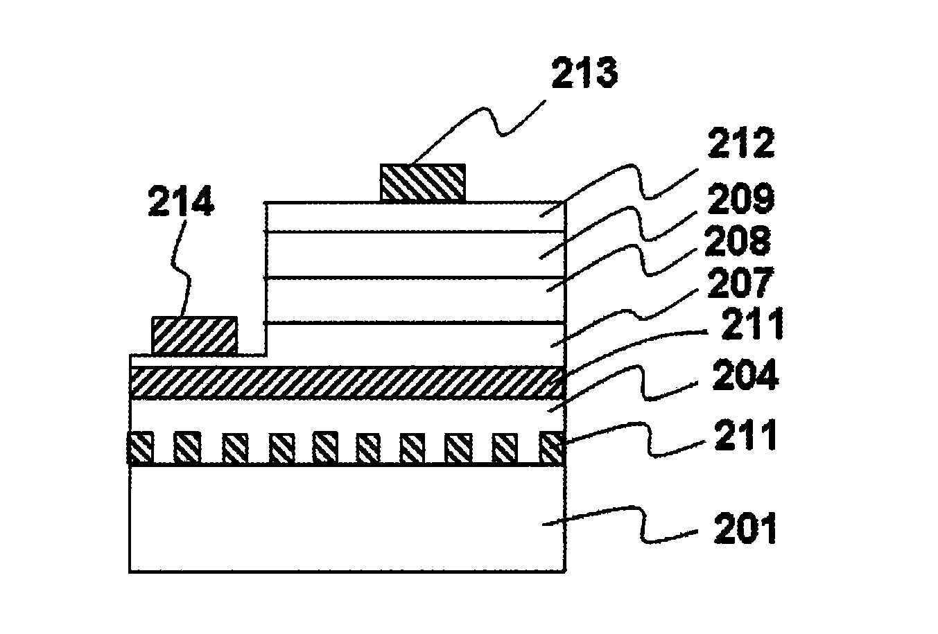
[0007]In order to solve the problem above in existing LEDs, an object of the present invention is to provide a GaN-based LED and a method for manufacturing the same. The present invention can effectively reduce the dislocation density in the epitaxial growth of the GaN-based layer, improve lattice quality, and have the advantage of improved the device performance and luminous efficiency.
[0022]Advantages of the present invention include: the two layers of cross-staggered through holes of the LED chips can effectively reduce the dislocation density in the epitaxial growth of the GaN-based layer, and improve lattice quality, device performance and luminous efficiency.

Problems solved by technology

However, for the popularization of semiconductor lighting, many problems are still left to be solved, among which the most important one lies in the production cost and luminous efficacy.
SiC substrates are expensive, resulting in high cost of LED production; and the lattice constant and coefficient of thermal expansion of sapphire are considerably different from those of GaN, causing a threading dislocation density of the GaN-based epitaxial layer as high as 108-1010 cm−2.
The high dislocation density may limit further improvement of the performance of the optoelectronic devices.
But due to the hardness of the sapphire substrate, it is difficult to ensure the consistency and uniformity of the patterns over the chip, which calls for high standard equipment and processing, and leads to high-priced PSS substrates and higher cost of LED production.
However, this method changes only the shape of the side of the epitaxial layer, and forms no through-hole structure, thus the improvement in light extraction is limited.

Method used


Image

  • GaN-Based Light-Emitting Diode and Method for Manufacturing the Same
  • GaN-Based Light-Emitting Diode and Method for Manufacturing the Same
  • GaN-Based Light-Emitting Diode and Method for Manufacturing the Same

Examples


Embodiment Construction

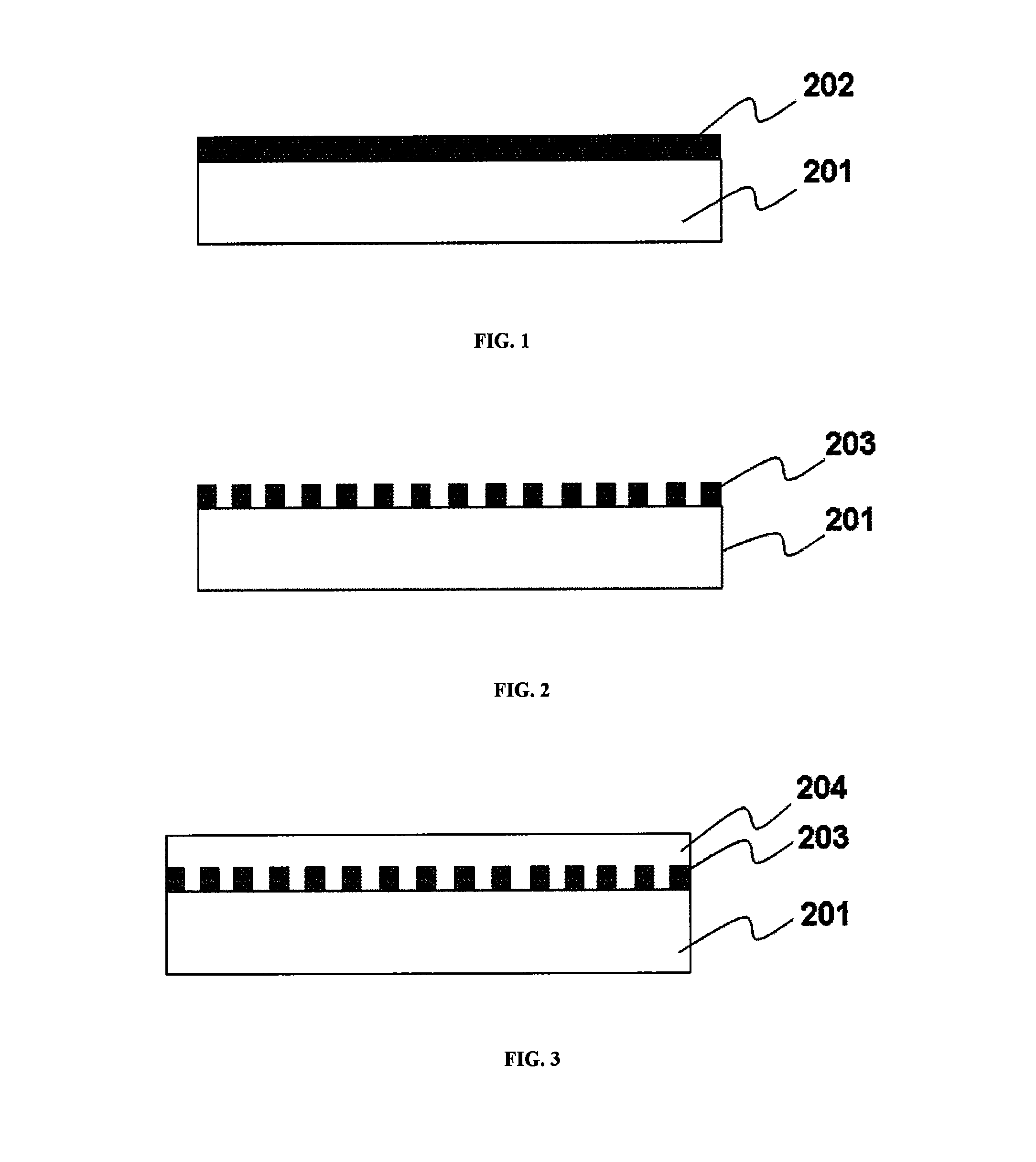
[0035]A method for manufacturing a GaN-based LED according to an embodiment the present invention is described hereinafter in conjunction with the accompanying drawings.

[0036]A first transition layer 202 is deposited on a sapphire substrate 201, as shown in FIG. 1. The material of the first transition layer may be one or more selected from a group consisting of SiO2, SiNx and TiO2.

[0037]A first patterned transition layer 203 with periodically distributed rectangles is formed by etching with a mask, as shown in FIG. 2 and FIG. 11.

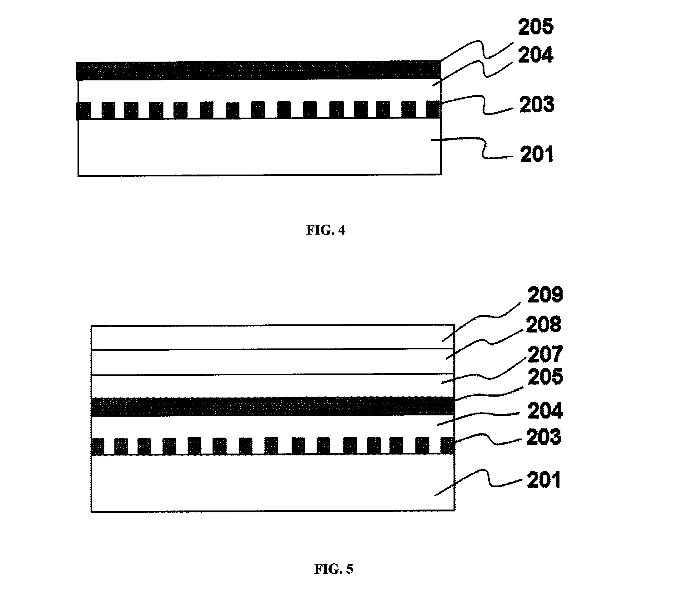
[0038]A first epitaxial layer is grown on the first patterned transition layer 203, and the first epitaxial layer includes a P—GaN layer 204, as shown in FIG. 3.

[0039]A second transition layer 205 is deposited on the first epitaxial layer 204, as shown in FIG. 4. The material of the second transition layer may be one or more selected from a group consisting of SiO2, SiNx and TiO2.

[0040]A second patterned transition layer 206 is formed by etching with a mask,...


PUM


Abstract

A GaN-based LED and a method for manufacturing the same are provided, and the method includes: providing a substrate, depositing a first transition layer on the substrate; forming a first patterned transition layer by etching with a mask; growing a first epitaxial layer on the first patterned transition layer; depositing a second transition layer on the first epitaxial layer; forming a second patterned transition layer by etching with a mask, such that the second patterned transition layer and the first patterned transition layer are cross-staggered with each other; growing a second epitaxial layer on the second patterned transition layer, wherein the second epitaxial layer includes a P-type layer, a light-emitting layer and an N-type layer; depositing a protection layer on the second epitaxial layer, dicing to obtain chips with a defined size; removing the first patterned transition layer and the second patterned transition layer on the substrate and the protection layer on the second epitaxial layer by wet etching, so as to form a structure with two layers of cross-staggered through holes; forming a conductive layer on the second epitaxial layer; and forming a P-electrode and an N-electrode by etching with a mask. The two layers of cross-staggered through holes of the LED chips can effectively reduce the dislocation density in the epitaxial growth of the GaN-based layer, and improve the lattice quality and luminous efficiency.

Description

CROSS REFERENCE TO RELATED APPLICATION[0001]This application claims the benefit of Chinese patent application 201010259995.5 filed Aug. 23, 2010 hereby incorporated by reference.FIELD OF THE INVENTION[0002]The present invention relates to a light-emitting diode, and in particular to a GaN-based light-emitting diode with two layers of staggered through holes and a method for manufacturing the same.BACKGROUND OF THE INVENTION[0003]A Light-Emitting Diode (LED) is a light-emitting semiconductor device based on the electroluminescence in the P—N junction of semiconductors. LEDs have the advantages including pollution-free, high brightness, low power consumption, long life cycle, low operating voltage, and easy to be small-scaled. Since the invention of gallium nitride (GaN) based LEDs in the 1990s, with the research progress, brightness has been continuously improved, and the range of application has become increasingly wider. With the continuous improvement in the efficiency of power Ga...

Claims


Application Information

Patent Timeline
Patent Type & Authority Applications(United States)
IPC IPC(8): H01L33/36
CPCH01L33/22H01L33/12
Inventor LIN, SU-HUIWU, JYH-CHIARNG
Owner XIAMEN SANAN OPTOELECTRONICS TECH CO LTD
Learn More