Compact, all solid-state, avalanche photodiode emitter-detector pixel with electronically selectable, passive or active detection mode, for large-scale, high resolution, imaging focal plane arrays

a photodiode emitter and pixel technology, applied in the field of compact, all solid-state, avalanche photodiode emitter detector pixel, can solve the problems of not being able to provide their own short-pulse laser illumination, unable to provide high-sensitivity detection light, and unable to provide short-pulse laser illumination. achieve the effect of high resolution

Inactive Publication Date: 2012-03-01
STERN ALVIN GABRIEL
View PDF3 Cites 34 Cited by
  • Summary
  • Abstract
  • Description
  • Claims
  • Application Information

AI Technical Summary

Benefits of technology

[0015]The hurdles associated with realizing a highly compact, monolithic, all solid-state imaging focal plane array having high resolution, as well as passive and active imaging capability, can be overcome using an advanced silico

Problems solved by technology

Focal plane arrays comprised of such linear or Geiger-mode silicon APD pixels, however, could only detect light with high sensitivity and were not in turn able to provide their own short pulse laser illumination at the pixel level, to an area in the scene spatially conjugated (using a camera lens for example) back to the respective pixel providing the illumination.
To date, no effective technology is available to allow the optical and electrical integration of a solid-state, laser light emitt

Method used


Image

  • Compact, all solid-state, avalanche photodiode emitter-detector pixel with electronically selectable, passive or active detection mode, for large-scale, high resolution, imaging focal plane arrays
  • Compact, all solid-state, avalanche photodiode emitter-detector pixel with electronically selectable, passive or active detection mode, for large-scale, high resolution, imaging focal plane arrays
  • Compact, all solid-state, avalanche photodiode emitter-detector pixel with electronically selectable, passive or active detection mode, for large-scale, high resolution, imaging focal plane arrays

Examples


Embodiment Construction

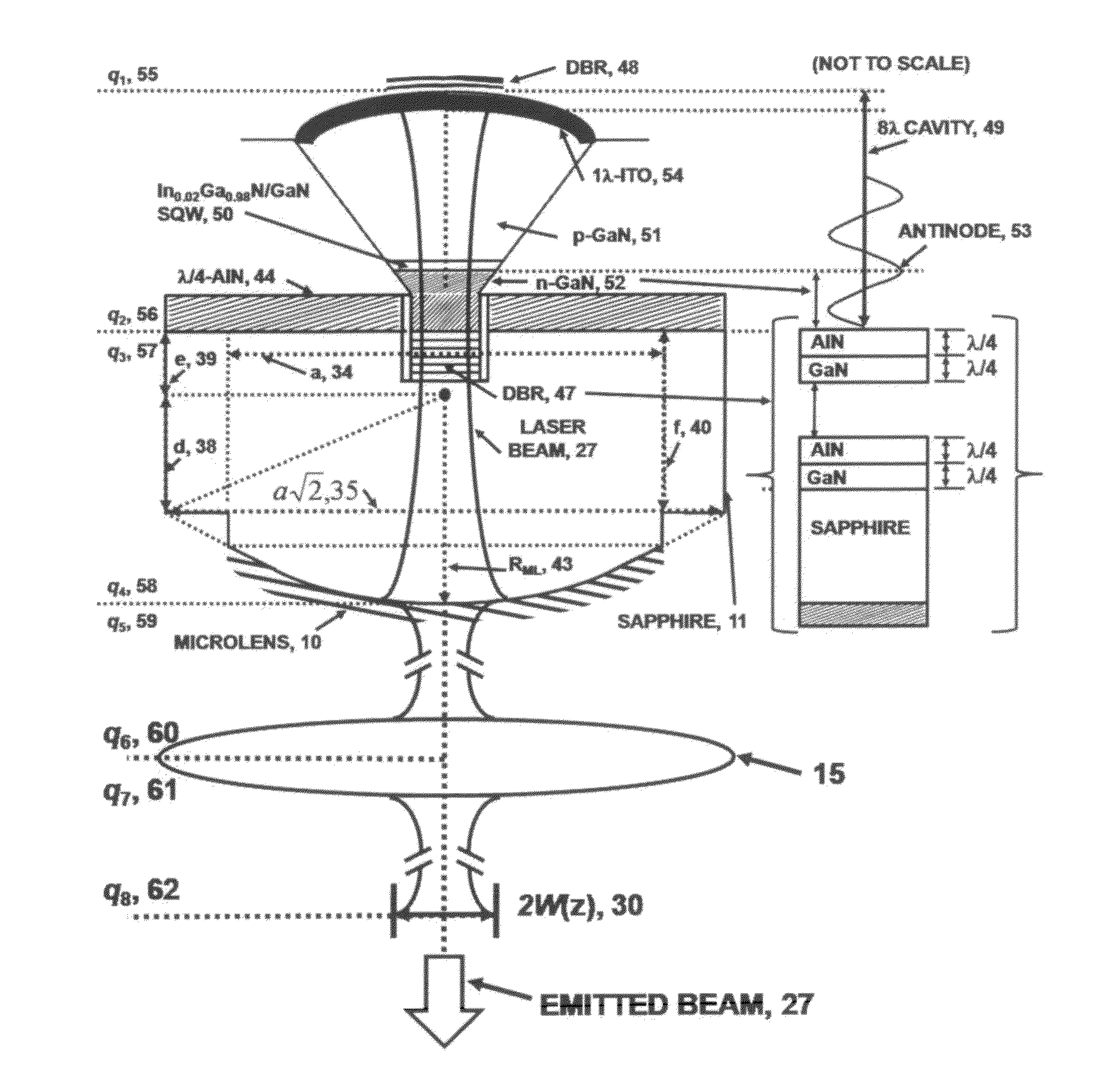
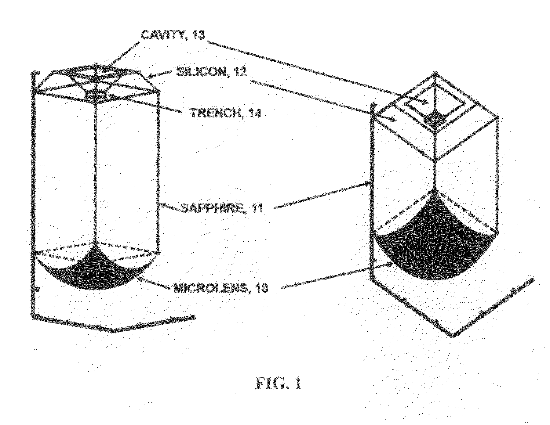
[0036]Referring to FIG. 1, a true scale depiction of the emitter-detector pixel is shown with sapphire microlens 10, sapphire substrate 11, anisotropically etched silicon APD detector mesa 12 with anisotropically etched, inverted mesa frustum shaped interior cavity 13 for the GaN / InGaN-VCSEL diode emitter. Also shown, is the trench 14 etched in the sapphire substrate for the front-side distributed Bragg reflector (DBR) of the VCSEL.

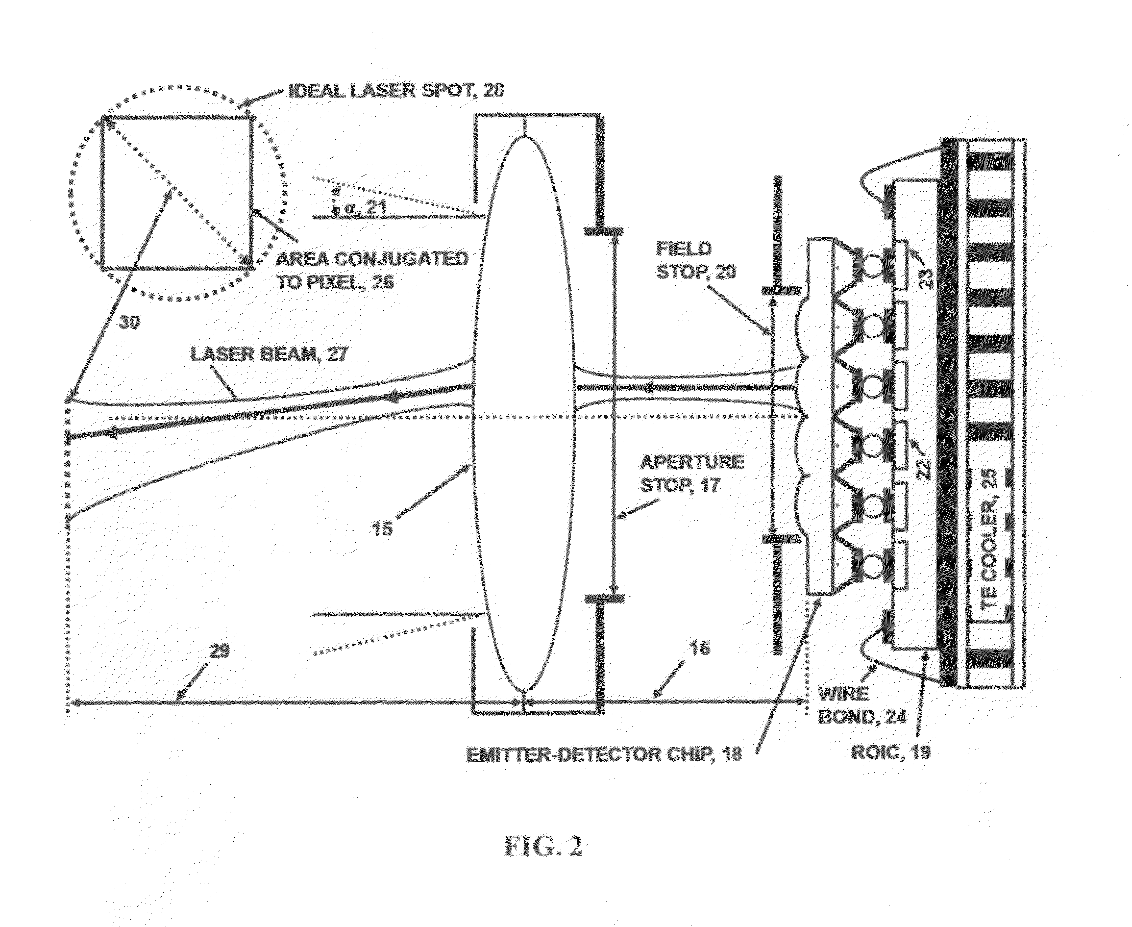
[0037]Referring to FIG. 2, the principal advantage of fabricating a solid-state laser diode in each pixel of the APD focal plane array imager is depicted where a highly compact; monolithic, all solid-state optical radar can be realized by use of a simple camera lens 15 with focal length F=0.21 meters 16, an aperture stop of diameter D=7.8 cm 17 and a focal plane array (FPA) consisting of an emitter-detector pixel array chip 18 that is flip-chip bump-bonded to a CMOS readout integrated circuit (ROIC) 19. The light sensitive, square area of the FPA sets the...


PUM


Abstract

An advanced, back-illuminated, silicon avalanche photodiode (APD) design is presented using silicon-on-sapphire with a novel crystalline aluminum nitride (AlN) antireflective layer between the silicon and R-plane sapphire. The substrate supports optical and electrical integration of a high quantum efficiency silicon APD with a gallium nitride (GaN)-VCSEL diode in each pixel to form a novel, compact, emitter-detector pixel for passive and active 2-D and 3-D high resolution, imaging focal plane arrays. Silicon mesa pixels are anisotropically etched with a central inverted mesa frustum cavity. The APD detector is fabricated in the silicon mesa and the GaN-VCSEL diode is grown epitaxially in the center of the mesa. A sapphire microlens below each pixel collimates the VCSEL beam and focuses optical returns into the APD detector. APDs share a common front-side anode, and VCSELs share a common cathode. The APD cathode is electrically connected to the VCSEL diode anode in each emitter-detector pixel.

Description

CROSS-REFERENCE TO RELATED APPLICATIONS[0001]Not ApplicableSTATEMENT REGARDING FEDERALLY SPONSORED RESEARCH OR DEVELOPMENT[0002]Not ApplicableREFERENCE TO SEQUENCE LISTING, A TABLE, OR A COMPUTER PROGRAM LISTING COMPACT DISC APPENDIX[0003]Not ApplicableBACKGROUND OF THE INVENTION[0004]For the purposes of imaging a scene, at low ambient illumination levels using a focal plane array comprised of solid-state detector devices, it is beneficial for the individual detectors in the array to be sensitive to light over a broad wavelength range and at single photon intensity levels. It would also be ideal if the focal plane array pixels were capable of providing their own source of short pulse, laser illumination to the area in the scene that is conjugated (using a camera lens for example) back to the respective pixel, providing the laser light pulse. Such an ideal solution would allow the solid-state detector pixels of the focal plane array to operate either in a conventional passive mode, c...

Claims


Application Information

Patent Timeline
IPC IPC(8): H01S5/026H01L21/77H01L27/146
CPCB82Y20/00H01L27/1464H01L27/14649H01L27/1465H01L31/107H01S5/0213H01S5/423H01S5/02415H01S5/0262H01S5/0425H01S5/18305H01S5/18388H01S5/34333H01S5/0218H01S5/0207H01S5/18358H01S5/04253H01S5/18341
Inventor STERN, ALVIN GABRIEL
Owner STERN ALVIN GABRIEL
Why Eureka
Try Eureka