Chip Attachment Layer Having Traverse-Aligned Conductive Filler Particles

a technology of conductive filler particles and conductive attachment layers, which is applied in the direction of layered products, transportation and packaging, chemistry apparatuses and processes, etc., can solve the problems of lowering the electrical conductivity of the attach layer and the electrical conductivity of the electrical conductivity, so as to reduce the electrical conductivity, the effect of lowering the electrical conductivity of the attach layer and reducing the electrical conductivity

Inactive Publication Date: 2012-05-03
TEXAS INSTR INC
View PDF1 Cites 13 Cited by
  • Summary
  • Abstract
  • Description
  • Claims
  • Application Information

AI Technical Summary

Benefits of technology

[0004]Applicant detected in microscopic analysis that during the phase of pressuring the chip onto the attach layer, the flowing adhesive resin causes the conductive filler particles throughout the layer to become horizontally oriented with respect to the chip/layer and substrate/layer interfaces. Applicant further found that the particles are wetted on all surfaces by the low-viscosity resin, inhibiting met

Problems solved by technology

Applicant further found that the particles are wetted on all surfaces by the low-viscosity resin, inhibiting metal-to-metal contact by surface tension and thus decreasing the electric

Method used


Image

  • Chip Attachment Layer Having Traverse-Aligned Conductive Filler Particles
  • Chip Attachment Layer Having Traverse-Aligned Conductive Filler Particles
  • Chip Attachment Layer Having Traverse-Aligned Conductive Filler Particles

Examples


Embodiment Construction

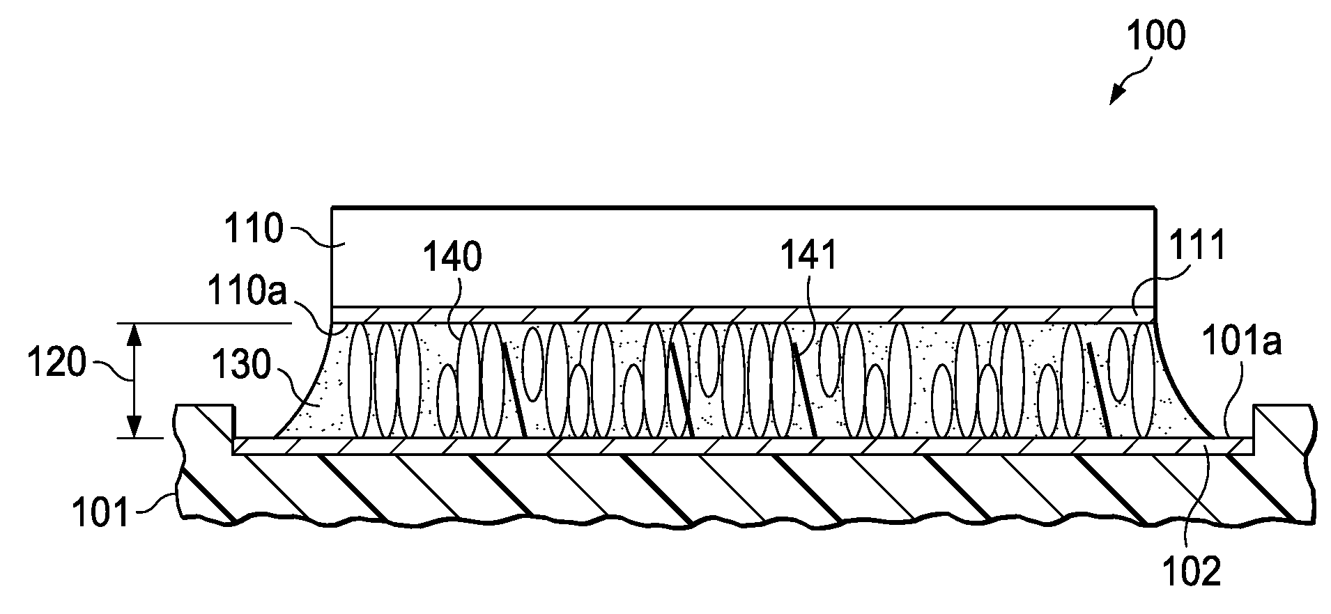
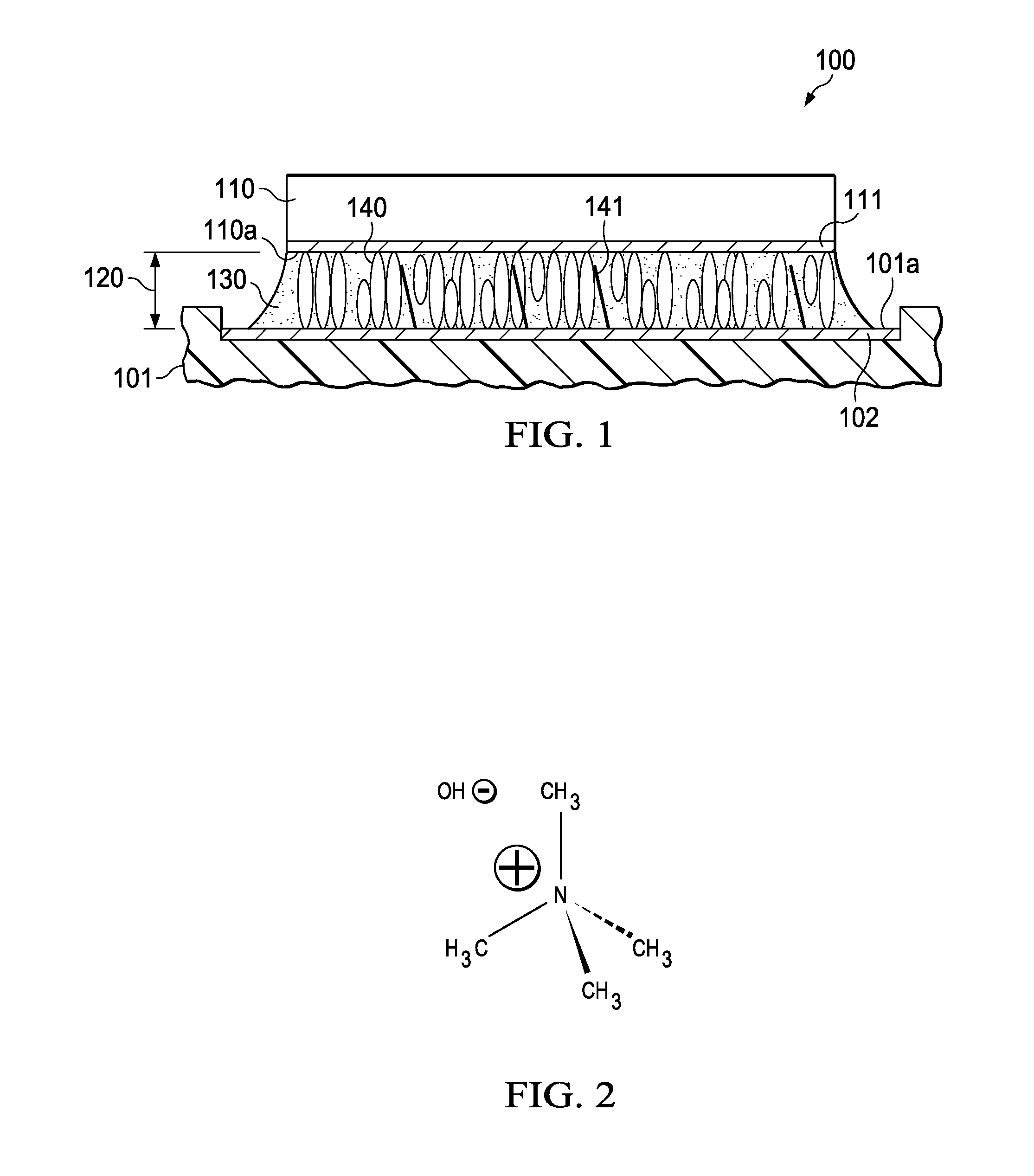
[0017]In a schematic cross section, FIG. 1 illustrates an exemplary device generally designated 100 assembled with an embodiment of the invention. Device 100 includes a substrate 101 and a workpiece 110. Substrate 101 may be an insulator, such as an FR-4 board, or a metal, such as a leadframe pad. Substrate 101 has a first surface 101a, which may be insulating or metallic, dependent on the material of the substrate. Preferably, surface 101a has good electrical and thermal conductivity; as sown in FIG. 1, an otherwise insulating substrate may have a metal inset 102 so that first surface 101a is actually the surface of the metal pad.

[0018]Workpiece 110 may be a semiconductor chip or any other piece part to be assembled on substrate 101. In either case, workpiece 110 may have a metal layer 111; for reasons of the invention to be discussed later (ferromagnetism), a preferred metal for layer 111 is nickel. Workpiece 110 has a second surface 110a. If workpiece 110 has metal layer 111, sec...


PUM

PropertyMeasurementUnit
Fractionaaaaaaaaaa
Fractionaaaaaaaaaa
Percent by massaaaaaaaaaa

Abstract

A method for conductively attaching a workpiece (110) onto a substrate (101). Spreading a layer of an adhesive polymeric compound (130) over the first surface (101a) of the substrate, the compound including a suspension of electrically and thermally conductive first particles (140) intermixed with a suspension of ferromagnetic surfactant-coated second particles (141). Applying an external magnetic field (401) to the layer, the field oriented normal to the first surface and capable of arraying the ferromagnetic particles in lines, and, by causality, aligning the conductive particles in chains normal to the first surface. Orienting the second surface (110a) of the workpiece parallel to the first substrate surface (101a) and bringing the aligned conductive particle chains (140) in contact with the first and second surfaces by pressing the workpiece onto the layer and piercing the chain ends to touch the first and second surfaces.

Description

FIELD OF THE INVENTION[0001]The present invention is related in general to the field of semiconductor devices and processes, and more specifically to the structure and fabrication method of chip attachment layers with traverse-aligned conductive filler particles.DESCRIPTION OF RELATED ART[0002]When semiconductor chips have to be attached to substrates or leadframes, it is common practice to use a layer of adhesive compound, such as an epoxy-based polymeric formulation, as a coupler between the chip and the substrate. The polymeric compound is usually a thermoset resin, applied to the chip attach pad of the substrate as a low-viscosity precursor to allow spreading of the compound over the attach pad. After the precursor resin is distributed, the chip is pressed onto the layer with a force sufficient to partially redistribute the adhesive by flowing and thus to ensure a uniform layer thickness across the whole chip area. Thereafter, the layer, together with the chip and the substrate,...

Claims


Application Information

Patent Timeline
IPC IPC(8): B32B5/16B32B38/00B32B7/00
CPCH01L2224/2936H01L2224/29357H01L2224/29439H01L2224/83009C09J9/02H01L24/29H01L24/32H01L24/83H01L2224/04026H01L2224/05655H01L2224/26175H01L2224/2929H01L2224/29339H01L2224/29355H01L2224/29393H01L2224/29499H01L2224/83192H01L2224/83851H01L2924/0665H01L2924/00014H01L2924/014H01L2924/00012H01L2224/32225H01L2224/32245C09J2203/326H01L2924/00H01L2224/325H01L2924/14Y10T428/24174
Inventor TELLKAMP, JOHN P.
Owner TEXAS INSTR INC
Why Eureka
Try Eureka