Electrical component and method for manufacturing electrical components

a technology of electrical components and components, applied in the direction of superimposed coating process, semiconductor/solid-state device details, transportation and packaging, etc., can solve the problems of short circuit, marked variation in the quality of the resulting electrical component, and the reduction of the solderability of the tin-plated film by heating

Inactive Publication Date: 2012-05-03
OM SANGYO
View PDF8 Cites 35 Cited by
  • Summary
  • Abstract
  • Description
  • Claims
  • Application Information

AI Technical Summary

Benefits of technology

[0019]In accordance with the present invention, there can be provided an electrical component having a surface...

Problems solved by technology

There has been, however, a problem that tin or a tin alloy without lead tends to form a whisker from a plated film and a grown whisker may cause short circuit.
A conventional heating process may, however, form an excessively thick diffusion layer between a superficial tin plated film and a base layer, leading to marked variation in quality of a resulting electrical component.
Furthermore, he...

Method used


Image

  • Electrical component and method for manufacturing electrical components
  • Electrical component and method for manufacturing electrical components
  • Electrical component and method for manufacturing electrical components

Examples


example 1

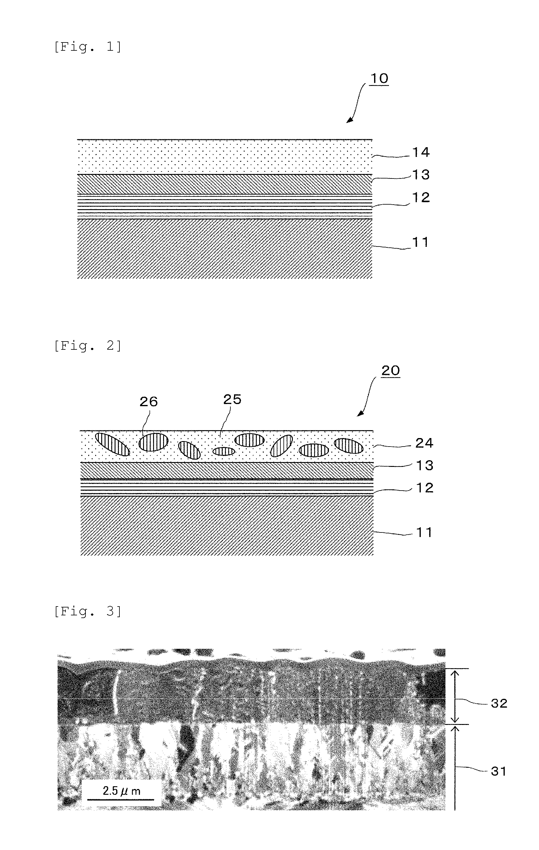
[0060]As a substrate, a phosphor bronze tape was used, in which a number of parts to be contacts for a connector are connected via a connecting member. This phosphor bronze tape was degreased and washed with an acid followed by copper strike plating (plating thickness: 0.1 μm) and then nickel plating (plating thickness: 2.0 μm) to form a base plated layer with a total thickness of about 2 μm, which was plated with palladium to give a middle plated layer with a thickness of 0.05 μm. The resulting middle plated layer was plated with tin to 3 μm to give a surface plated layer with a thickness of about 3 μm. Each of these plating processes was conducted by hoop plating, in which a palladium plating solution was PD-LF-800 from N. E. Chemcat. Corporation and a tin plating solution was SBS-M from Yuken Industry Co., Ltd. Thus, tape 1 having a number of contacts for a connector, as an electrical component of the present invention, connected to the tape was obtained. That is, tape 1 has the ...

example 2

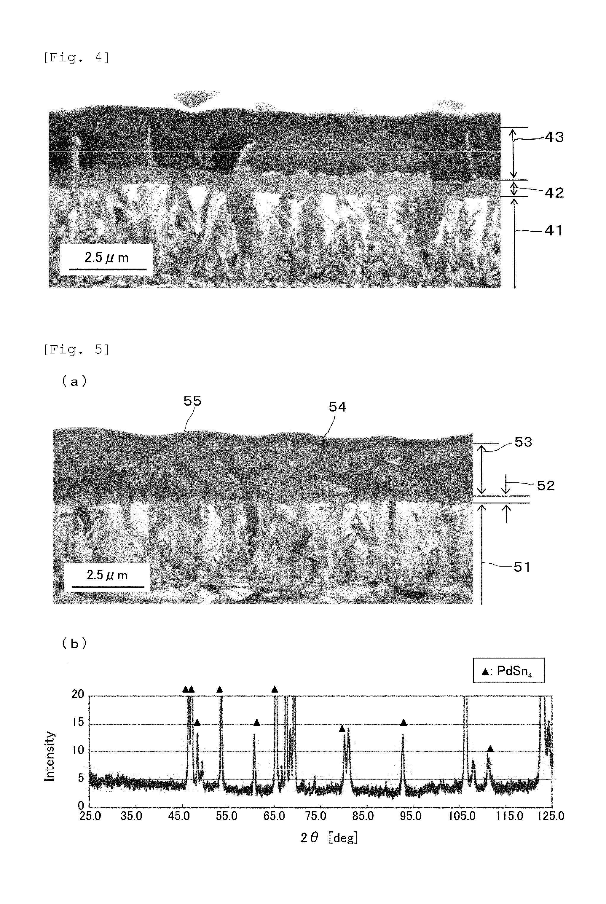
[0062]Tape 1 produced in Example 1 was placed in a simple reflow oven and annealed at a peak temperature of 225° C. for 2 min to give tape 2. The cross-section of tape 2 thus produced was observed as described in Example 1. FIG. 4 shows a microgram of the cross-section of the observed part. In FIGS. 4, 41, 42 and 43 indicate a nickel base layer, a diffusion layer as a middle layer and a tin surface layer, respectively.

example 3

[0063]Tape 1 produced in Example 1 was placed in a portable reflow oven and reflowed at a peak temperature of 310° C. for 2 sec to give tape 3. The cross-section of tape 3 thus produced was observed as described in Example 1. FIG. 5(a) shows a microgram of the cross-section of the observed part. In FIGS. 5(a), 51, 52 and 53 indicate a nickel base layer, a tin-palladium diffusion layer as a middle layer and a surface layer, respectively. In the surface layer 53, 54 is a tin phase and 55 is a tin-palladium alloy phase. Furthermore, the surface of tape 3 was observed by an X-ray diffractometer. FIG. 5(b) shows the X-ray diffraction pattern obtained. Thus, the presence of a peak corresponding to PdSn4 was confirmed.

[0064]In Example 2, it was demonstrated that annealing after forming each plated layer allowed for forming the diffusion layer 42 between the surface layer43 and the base layer 41. In Example 2, it was also demonstrated that the diffusion layer 42 was formed under the tin sur...


PUM

PropertyMeasurementUnit
Thicknessaaaaaaaaaa
Angleaaaaaaaaaa
Molar densityaaaaaaaaaa

Abstract

An electrical component is provided by a method comprising forming a middle plated layer made of palladium or a palladium alloy on a substrate and forming a surface plated layer made of tin or a tin alloy containing a metal other than palladium on the middle plated layer. Thus, there can be provided an electrical component having a surface layer consisting primarily of tin in which whisker formation can be prevented for a long period under stress.

Description

TECHNICAL FIELD[0001]The present invention relates to an electrical component having a plated layer made of tin or a tin alloy on the surface of a substrate and a manufacturing method therefor. In particular, the present invention relates to an electrical component such as a terminal, a connector and a flexible substrate for flip-chip mounting and a manufacturing method therefor, in which whisker formation from the plated layer can be prevented.BACKGROUND ART[0002]Generally, an alloy consisting primarily of tin is plated on the surface of an electrical component such as a terminal, a connector, a lead frame in a semiconductor integrated circuit for preventing oxidation, reducing a contact resistance and improving solderability. Such an alloy for plating has been suitably a tin-lead alloy. However, needs for lead-free electrical and electronic components have accelerate investigations for plating with tin alone or a lead-free alloy such as tin-silver, tin-bismuth and tin-copper. Ther...

Claims


Application Information

Patent Timeline
IPC IPC(8): B05D5/12H01L29/12C23C28/02
CPCC25D3/30C25D3/50C25D3/60C25D5/10C25D5/12C25D5/48C25D5/50H01L23/49582H01R13/03H01L2924/0002H01L2924/00Y10T428/12528C25D5/617
Inventor TAKAMIZAWA, MASAONAKA, TOSHIHIDEKEMMOTSU, HITOSHINISHIMURA, YOSHIYUKI
Owner OM SANGYO
Why Eureka
Try Eureka