Structure and method for enhancing interfacial perpendicular anisotropy in CoFe(B)/MgO/CoFe(B) Magnetic Tunnel Junctions

a technology of magnetic tunnel junction and perpendicular anisotropy, which is applied in the direction of magnetic materials for record carriers, magnetic bodies, instruments, etc., can solve the problems of destroying a thin tunnel barrier made of alox, mgo, etc., and affecting the performance of the magnetic tunnel junction, so as to reduce the undesirable soft breakdown component

Active Publication Date: 2012-05-31
TAIWAN SEMICON MFG CO LTD
View PDF9 Cites 98 Cited by
  • Summary
  • Abstract
  • Description
  • Claims
  • Application Information

AI Technical Summary

Benefits of technology

[0018]A second objective of the present invention is to provide a MTJ according to the first objective that also reduces the undesirable soft breakdown (SBD) component of Vbd (breakdown voltage) to <0.1%.

Problems solved by technology

As the size of MRAM cells decreases, the use of external magnetic fields generated by current carrying lines to switch the magnetic moment direction becomes problematic.
This high current density, which is required to induce the spin-transfer effect, could destroy a thin tunnel barrier made of AlOx, MgO, or the like.

Method used


Image

  • Structure and method for enhancing interfacial perpendicular anisotropy in CoFe(B)/MgO/CoFe(B) Magnetic Tunnel Junctions
  • Structure and method for enhancing interfacial perpendicular anisotropy in CoFe(B)/MgO/CoFe(B) Magnetic Tunnel Junctions
  • Structure and method for enhancing interfacial perpendicular anisotropy in CoFe(B)/MgO/CoFe(B) Magnetic Tunnel Junctions

Examples


second embodiment

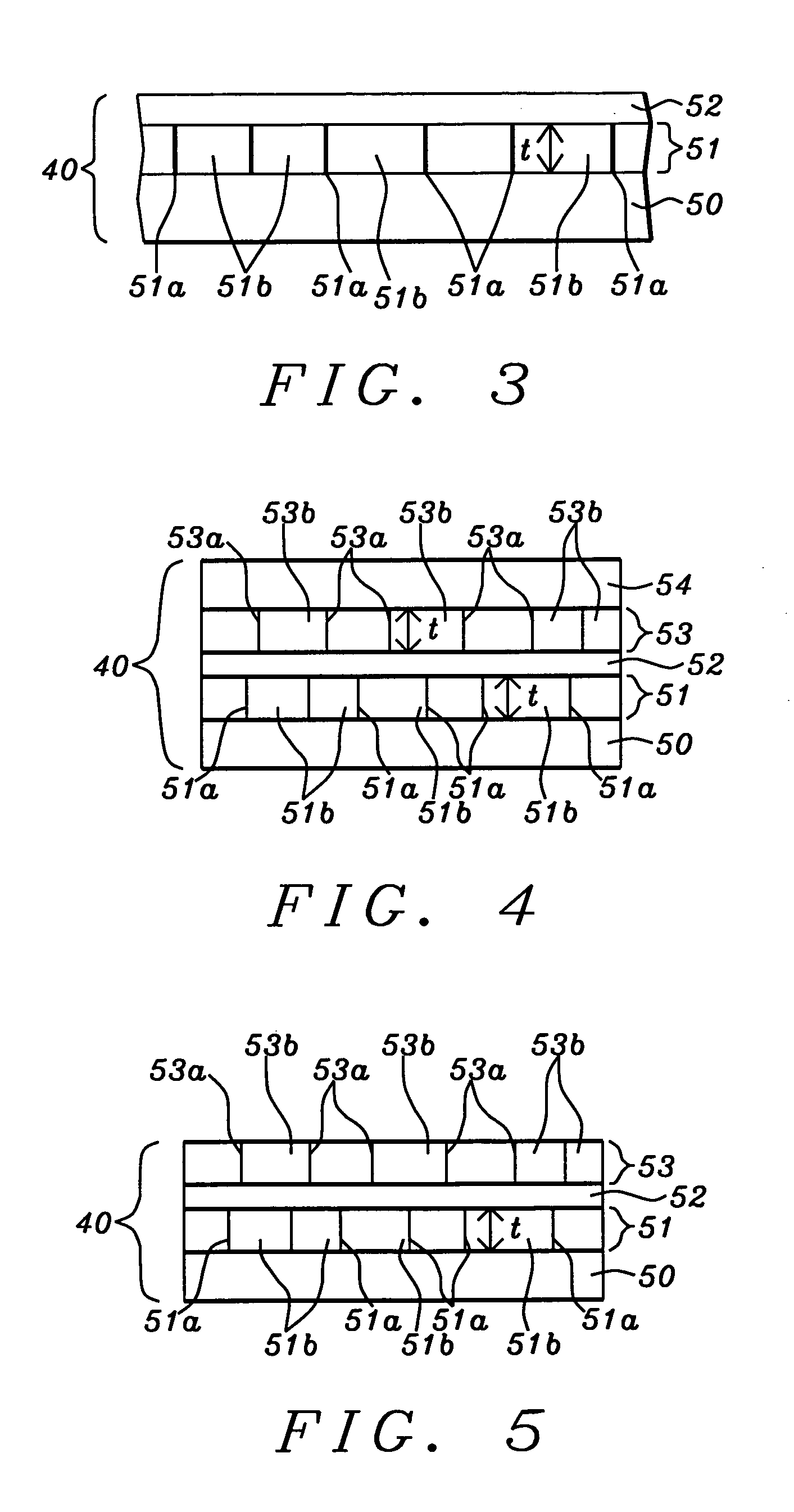
[0054]Referring to FIG. 4, second embodiment of the present invention is depicted that may be referred to as a dual NCC free layer. In particular, the dual NCC free layer 40 configuration in the MTJ stack (FIG. 2) comprises the NCC free layer structure shown in FIG. 3 and an additional second NCC layer 53 and third magnetic (FL3) layer 54 sequentially formed on FL2 layer 52 to give a FL1 / NCC / FL2 / NCC / FL3 structure. In the exemplary embodiment, each of the NCC layers 51, 53 has a thickness from 4 to 6 Angstroms, and preferably 5 Angstroms. The dual NCC configuration has an overall NCC thickness (NCC 51+NCC 53) greater than for a single NCC layer 51 which is typically around 8 Angstroms. Note that NCC layer 53 may be comprised of the same R(M) grains formed in a metal (M) oxide, nitride, or oxynitride insulator matrix previously described with respect to NCC layer 51. Thus, more heat is generated in the granular R(M) columns 51a, 53a for thermally assisting a switch in free layer 40 ma...

third embodiment

[0055]Referring to FIG. 5, the present invention is illustrated and retains all of the features of the dual NCC layer in the previous embodiment except the upper FL3 layer 54 is omitted and the free layer 40 has a FL1 / NCC1 / FL2 / NCC2 configuration. In this case, upper NCC2 layer 53 is the top layer in the free layer stack instead of a FL2 or FL3 layer as in previous embodiments. Preferably, the thickness of FL1 layer 50 is from 14.5 to 15.5 Angstroms and the thickness of FL2 layer 52 is from 6 to 8.5 Angstroms. Both of NCC1 51 and NCC2 53 layers have a thickness from 4 to 6 Angstroms, and preferably 6 Angstroms.

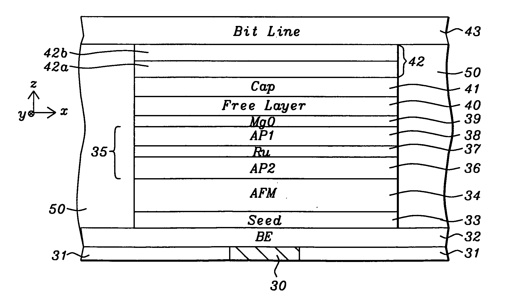
[0056]Returning to FIG. 2, a cap layer 41 is formed on free layer 40 and may be comprised of Ru having a thickness of 10 to 30 Angstroms, and preferably 30 Angstroms. In another embodiment, one or more other metals such as Ta may be employed as a capping layer either as a single layer, an alloy layer, a composite layer comprised of a stack of two or more metal layers, or in com...


PUM

PropertyMeasurementUnit
thicknessaaaaaaaaaa
thicknessaaaaaaaaaa
thicknessaaaaaaaaaa

Abstract

A STT-RAM MTJ is disclosed with a MgO tunnel barrier formed by natural oxidation process. A Co10Fe70B20 / NCC / Co10Fe70B20, Co10Fe70B20 / NCC / Co10Fe70B20 / NCC, or Co10Fe70B20 / NCC / Co10Fe70B20 / NCC / Co10Fe70B20 free layer configuration where NCC is a nanocurrent channel layer made of Fe(20%)-SiO2 is used to minimize Jc0 while enabling higher thermal stability, write voltage, read voltage, Ho, and Hc values that satisfy 64 Mb design requirements. The NCC layer is about 10 Angstroms thick to match the minimum Fe(Si) grain diameter size. The MTJ is annealed with a temperature of about 330° C. to maintain a high magnetoresistive ratio while maximizing Hk⊥(interfacial) for the free layer thereby reducing Heff and lowering the switching current. The Co10Fe70B20 layers are sputter deposited with a low pressure process with a power of about 15 Watts and an Ar flow rate of 40 standard cubic centimeters per minute to lower Heff for the free layer.

Description

RELATED PATENT APPLICATION[0001]This application is related to the following: Docket # HMG08-043 / 09-006, Ser. No. 12 / 460,412, filing date Jul. 17, 2009; which is assigned to a common assignee and is herein incorporated by reference in its entirety.FIELD OF THE INVENTION[0002]The invention relates to a high performance Magnetic Tunneling Junction (MTJ) element and a method for making the same, and in particular, to a spin transfer torque (STT-RAM) device that achieves low switching current and high dR / R by incorporating a free layer having a FL1 / NCC / FL2 or FL1 / NCC / FL2 / NCC / FL3 configuration in which a nanocurrent channel (NCC) layer magnetically and electrically couples adjoining ferromagnetic layers FL1 and FL2 in a single NCC structure or FL1, FL2, and FL3 ferromagnetic layers in a dual NCC structure.BACKGROUND OF THE INVENTION[0003]Magnetoresistive Random Access Memory (MRAM), based on the integration of silicon CMOS with MTJ technology, is a major emerging technology that is highl...

Claims


Application Information

Patent Timeline
Patent Type & Authority Applications(United States)
IPC IPC(8): G11B5/706B05D5/00C23C14/34
CPCC23C14/3414H01F10/3272H01F10/3286G11C11/161H01F41/307Y10T428/1114H01L43/12H01F10/3295H01F10/3259B82Y40/00H01L43/08H10N50/10H10N50/01
Inventor HORNG, CHENG T.TONG, RU-YINGJAN, GUENOLE
Owner TAIWAN SEMICON MFG CO LTD
Why Eureka
Try Eureka