

Fluorescence emissions detector
a technology of fluorescence emission and detection circuit, which is applied in the direction of fluorescence/phosphorescence, luminescent dosimeter, optical radiation measurement, etc., can solve the problems of undesired crosstalk in the detection system, and achieve the effect of reducing the gain of the first amplifier stage, minimizing the effect of charge injection, and substantially the same effective input resistance and capacitan
- Summary
- Abstract
- Description
- Claims
- Application Information
AI Technical Summary
Benefits of technology
Problems solved by technology
Method used
Image

Examples
Embodiment Construction
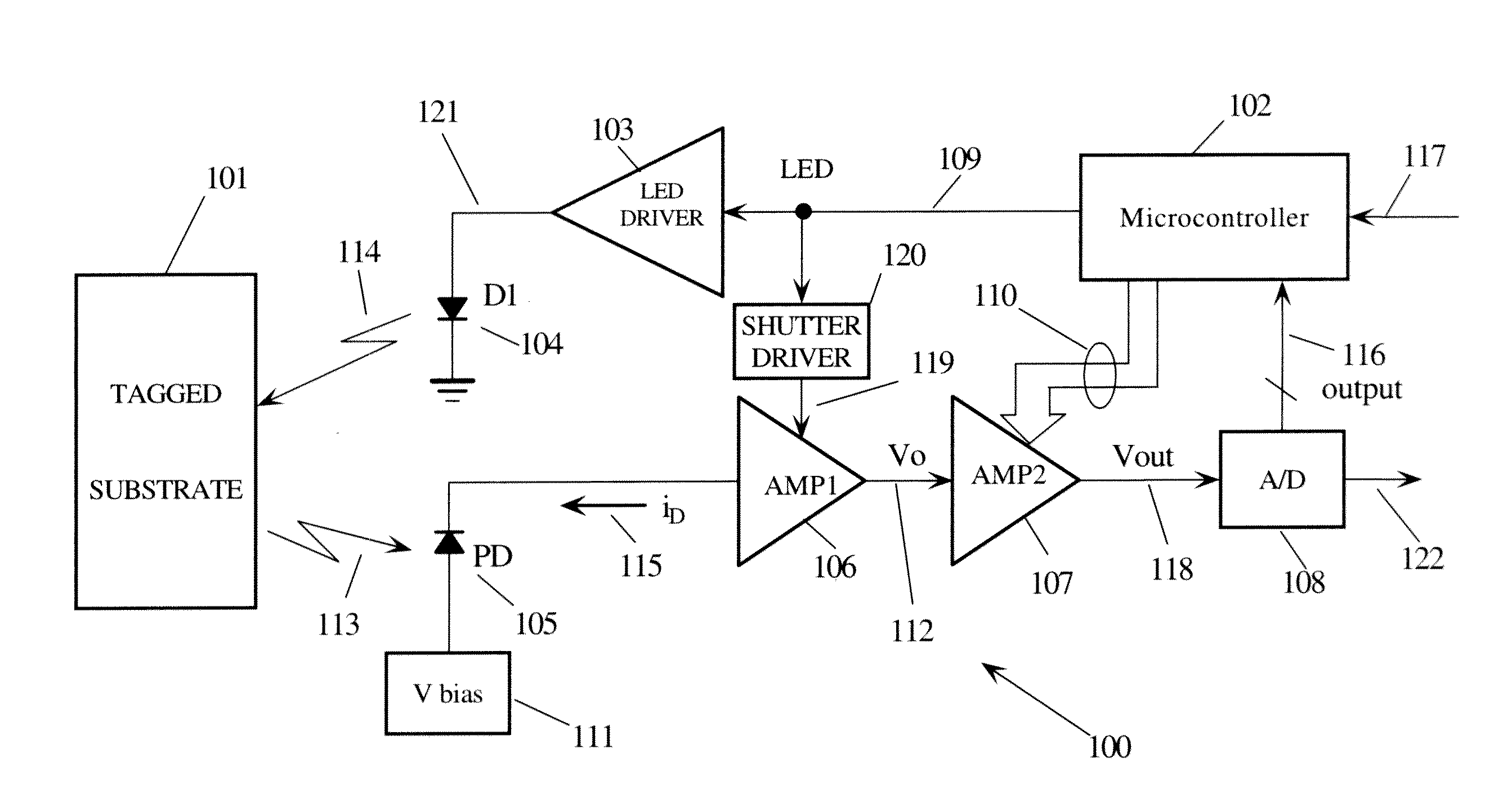
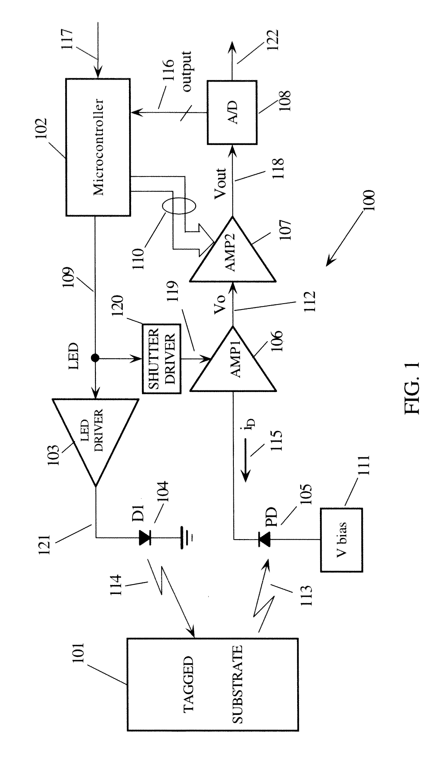
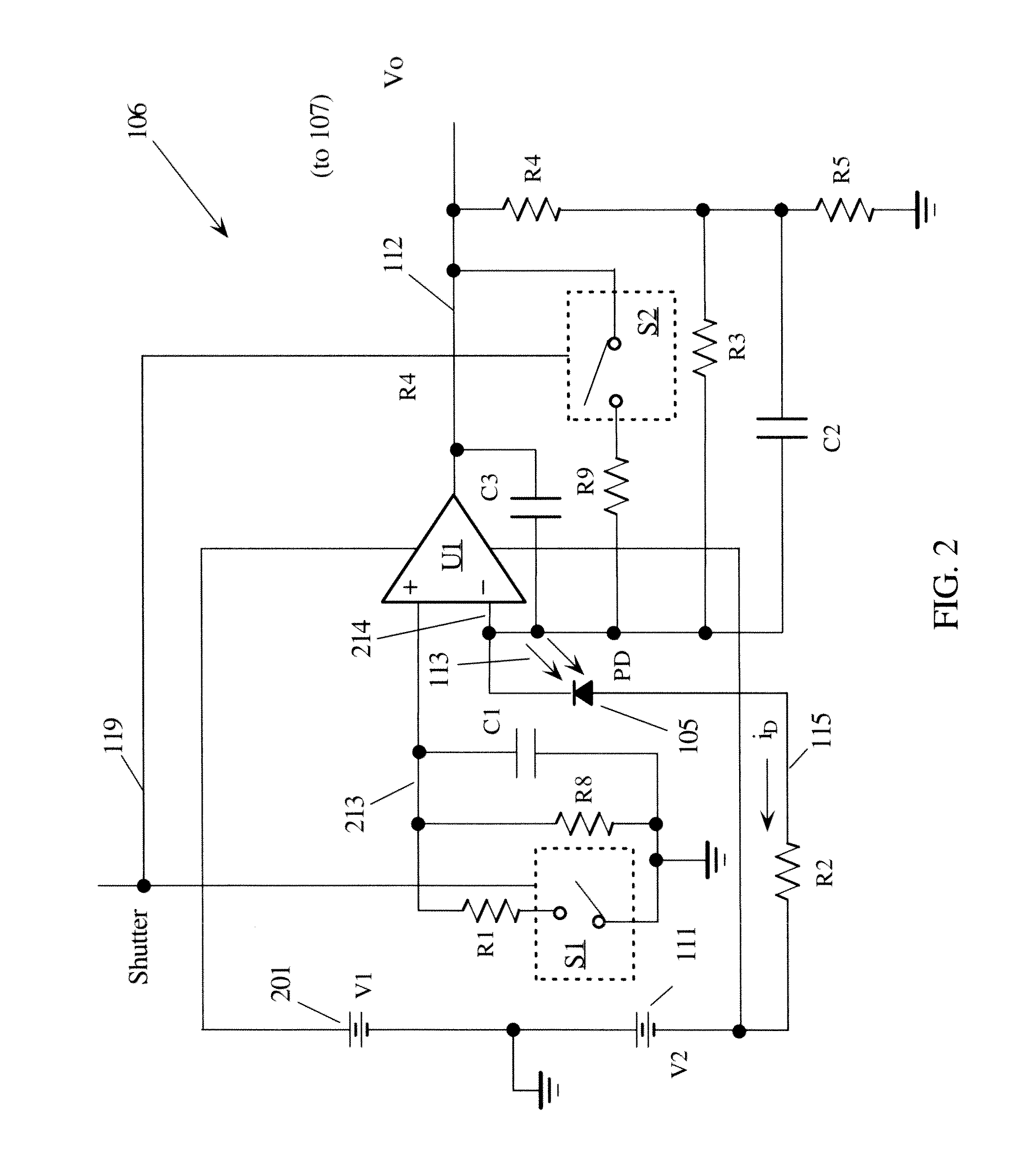
[0014]The analog front end of a single element resonant fluorescence detection system comprises an excitation circuit and a single photodiode connected to a photodiode amplifier. The analog front end (AFE) establishes a maximum performance of the system with regards to bandwidth, signal-to-noise ratio, linearity, and dynamic range. The output comprises a decaying exponential voltage that is the analog of a resonant fluorescence signal with minimal distortion due to instrumental artifacts and overlapping spectra.
[0015]Fluorescence is the emission of electromagnetic radiation or light immediately after absorbing incident radiation or light. The resonant fluorescence phenomenon occurs when the spectra or wavelength of the emission overlaps the incident or excitation source wavelength. The delay time between absorption and emission is minimal. The fluorescence lifetime or 1 / e value is the time that is equivalent to 36.8% of the initial intensity value of the fluorescing signal.
[0016]The...
PUM
 Abstract
Description
Claims
Application Information