Silicon nitride film and process for production thereof, computer-readable storage medium, and plasma CVD device
- Summary
- Abstract
- Description
- Claims
- Application Information
AI Technical Summary
Benefits of technology
Problems solved by technology
Method used
Image

Examples
first embodiment
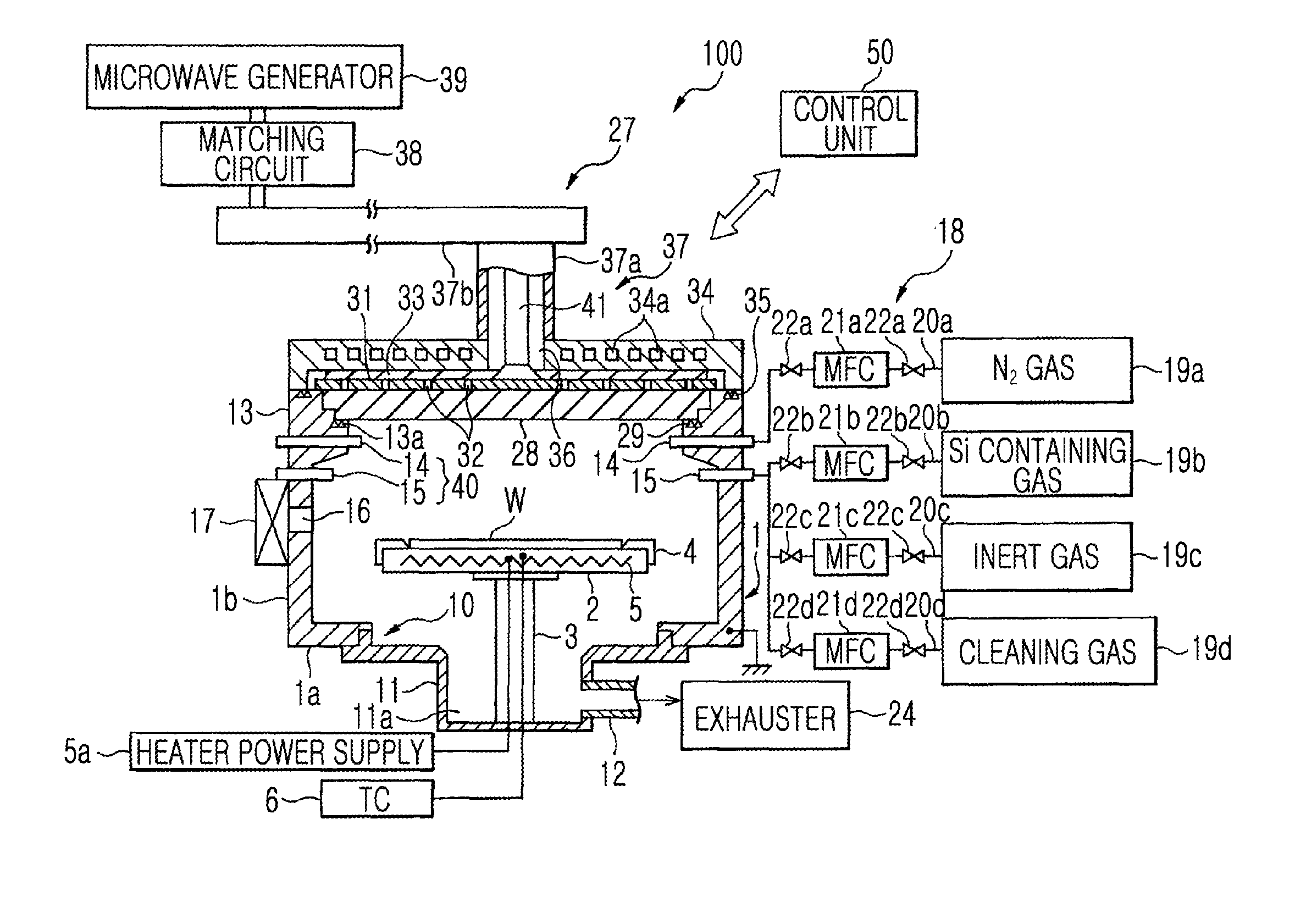
[0040]Hereinafter, the present invention will be described in detail by explaining exemplary embodiments of the invention with reference to the attached drawings. FIG. 1 is a schematic cross-sectional view showing a schematic structure of a plasma CVD device 100 used in a process for production of a silicon nitride film according to the present invention.
[0041]The plasma CVD device 100 is configured as a RLSA (Radial Line Slot Antenna) microwave plasma process apparatus that can generate microwave excitation plasma having a high density and a low electron temperature, by generating plasma by introducing microwaves into a process chamber by using a planar antenna including a plurality of apertures each having a slot shape, specifically a RLSA. The plasma CVD device 100 is able to perform a process using plasma having a low electron temperature from 0.7 eV to 2 eV, and a plasma density from 1×10¹⁰ / cm3 to 5×10¹² / cm3. Accordingly, the plasma CVD device 100 may be very suitably used to f...
PUM
| Property | Measurement | Unit |
|---|---|---|
| Fraction | aaaaa | aaaaa |
| Fraction | aaaaa | aaaaa |
| Fraction | aaaaa | aaaaa |
Abstract
Description
Claims
Application Information
 - Generate Ideas
- Intellectual Property
- Life Sciences
- Materials
- Tech Scout
- Unparalleled Data Quality
- Higher Quality Content
- 60% Fewer Hallucinations
Browse by: Latest US Patents, China's latest patents, Technical Efficacy Thesaurus, Application Domain, Technology Topic, Popular Technical Reports.
© 2025 PatSnap. All rights reserved.Legal|Privacy policy|Modern Slavery Act Transparency Statement|Sitemap|About US| Contact US: help@patsnap.com