

Adhesive film, multilayer circuit board, electronic component and semiconductor device
a multi-layer circuit board and adhesive film technology, applied in the direction of film/foil adhesives without carriers, film/foil adhesives, final product manufacturing, etc., can solve the problems of difficult to secure the reliability of electronic components and semiconductor devices, and difficult to secure insulation properties between adjacent terminals, so as to achieve excellent electrical connectivity and insulation reliability.
- Summary
- Abstract
- Description
- Claims
- Application Information
AI Technical Summary
Benefits of technology
Problems solved by technology
Method used
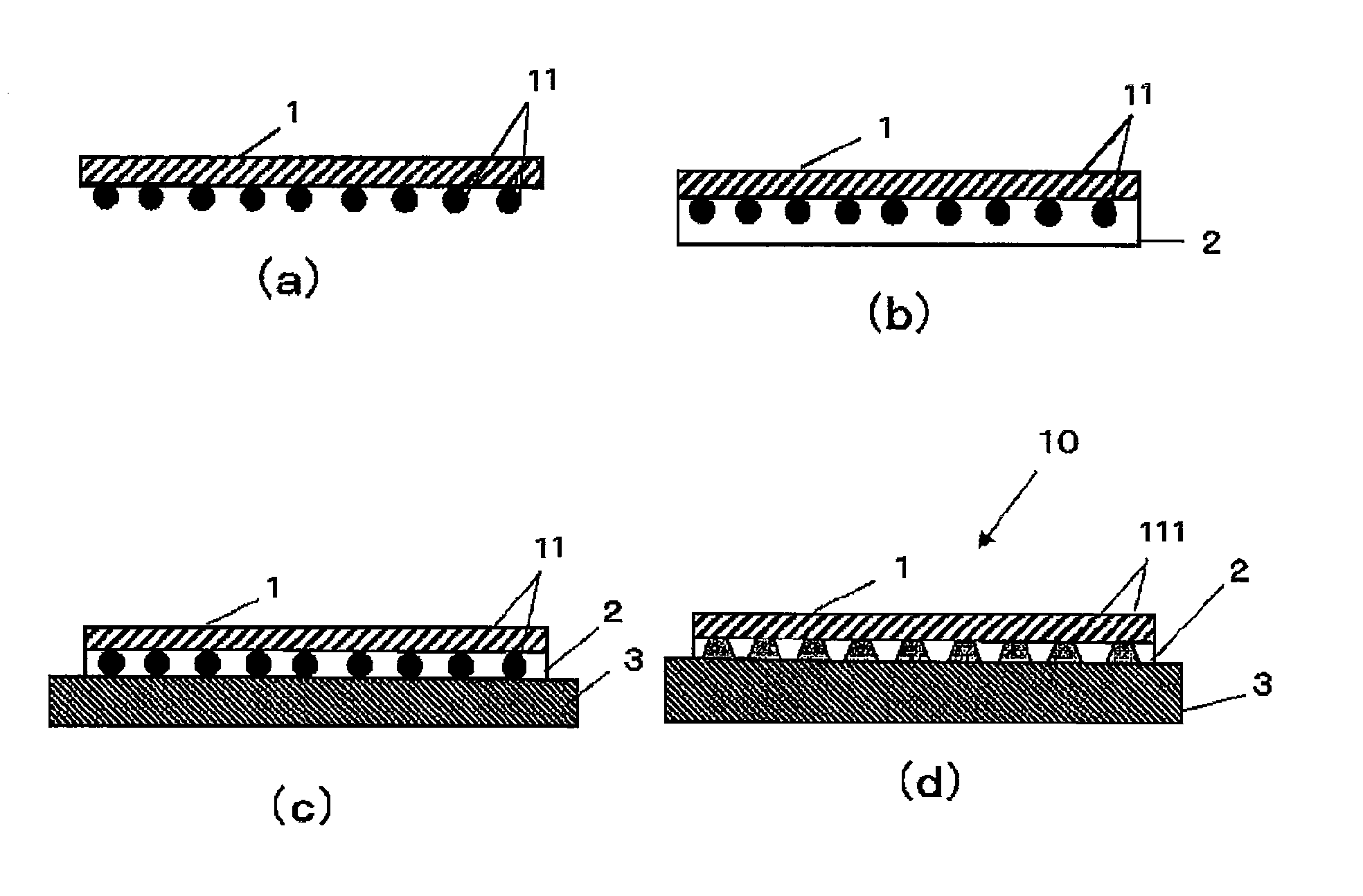
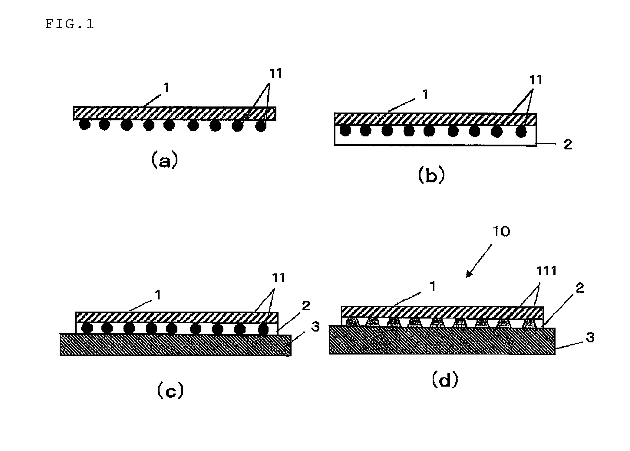
Image

Examples
example 1
Preparation of Varnish for Adhesive Film
[0124]55.0 weight parts of a bisphenol F type epoxy resin (EPICLON-830LVP, commercially available from DIC Corporation) as the thermosetting resin (A), 30.8 weight parts of a phenol novolac resin (VR-9305, commercially available from Mitsui Chemicals, Inc.) as the curing agent (B), 3.0 weight parts of sebacic acid (a product of Tokyo Chemical Industry, Co., Ltd.) as the compound having flux activity (C), 10.0 weight parts of a bisphenol F type phenoxy resin (YP-70, commercially available from Tohto Kasei Co., Ltd.) as the film forming resin (D), 0.2 weight parts of 2-phenyl-4-methylimidazole (2P4MZ, commercially available from Shikoku Chemicals Corp.) as the curing accelerator (E), and 1.0 weight part of β-(3,4-epoxycyclohexyl)ethyltrimethoxysilane (KBM-303, commercially available from Shin-Etsu Chemical Co., Ltd.) as the silane coupling agent (F) were dissolved in methyl ethyl ketone, whereby a resin varnish having a resin concentration of 50...
example 2
Preparation of Varnish for Adhesive Film
[0132]An adhesive film and a semiconductor device were prepared in the same manner as in Example 1, except that 50.0 weight parts of a bisphenol A type epoxy resin (EPICLON-840S, commercially available from DIC Corporation) as the thermosetting resin (A), 25.5 weight parts of a phenol novolac resin (VR-9305, commercially available from Mitsui Chemicals, Inc.) as the curing agent (B), 3.0 weight parts of sebacic acid (a product of Tokyo Chemical Industry, Co., Ltd.) as the compound having flux activity (C), 20.0 weight parts of a bisphenol F type phenoxy resin (YP-70, commercially available from Tohto Kasei Co., Ltd.) as the film forming resin (D), 0.5 weight parts of 2-phenyl-4-methylimidazole (2P4MZ, commercially available from Shikoku Chemicals Corp.) as the curing accelerator (E), and 1.0 weight part of β-(3,4-epoxycyclohexyl)ethyltrimethoxysilane (KBM-303, commercially available from Shin-Etsu Chemical Co., Ltd.) as the silane coupling age...
example 3
Preparation of Varnish for Adhesive Film
[0133]An adhesive film and a semiconductor device were prepared in the same manner as in Example 1, except that 20.0 weight parts of a cresol novolac type epoxy resin (EOCN-1020-70, commercially available from Nippon Kayaku Co., Ltd.) as the thermosetting resin (A), 15.0 weight parts of a phenol novolac resin (PR55617, commercially available from Sumitomo Bakelite Co., Ltd.) as the curing agent (B), 3.0 weight parts of sebacic acid (a product of Tokyo Chemical Industry, Co., Ltd.) as the compound having flux activity (C), 60.0 weight parts of a bisphenol A type phenoxy resin (YP-50, commercially available from Tohto Kasei Chemical Co., Ltd.) as the film forming resin (D), 1.0 weight part of 2-phenyl-4-methylimidazole (2P4MZ, commercially available from Shikoku Chemicals Corp.) as the curing accelerator (E), and 1.0 weight part of β-(3,4-epoxycyclohexyl)ethyltrimethoxysilane (KBM-303, commercially available from Shin-Etsu Chemical Co., Ltd.) as...
PUM
| Property | Measurement | Unit |
|---|---|---|
| Fraction | aaaaa | aaaaa |
| Percent by mass | aaaaa | aaaaa |
| Percent by mass | aaaaa | aaaaa |
Abstract
Description
Claims
Application Information