Method for filling a gap

a gap and gap technology, applied in the field of semiconductor technology, can solve the problems of affecting the reliability of devices, more difficulty in filling structures by electroplating, and voids in filled through-holes, so as to reduce or eliminate the possibility of producing voids and increase the reliability of circuits

Inactive Publication Date: 2012-07-26
INST OF MICROELECTRONICS CHINESE ACAD OF SCI
View PDF11 Cites 10 Cited by
  • Summary
  • Abstract
  • Description
  • Claims
  • Application Information

AI Technical Summary

Benefits of technology

[0026]In an embodiment of the invention, a method for filling a gap is provided. In the method, a diffusion barrier layer and a seed layer are formed sequentially in the gap and on the surface of the insulating dielectric layer outside the gap. And there is a mask layer formed on the surface of the seed layer outside the gap. Due to the suppression effect of the mask layer, the subsequent plating of Cu is not performed on the surface area in and outside the gap simultaneously. Instead, the metal layer is first deposited in the gap and then on the surface outside the gap, which can avoid the phenomenon of overhang, reduce or eliminate the possibility to produce voids, and hence increase the reliability of the circuits.

Problems solved by technology

However, the operation speed of chips is obviously influenced by Resistance Capacitance Delay Time (RC Delay Time) caused by metal lines.
Currently, with the continuous scaling down of devices, sizes of semiconductor structures become smaller and smaller, resulting in more difficulty in filling a structure by electroplating.
The overhang may be enlarged in the process of electroplating, which finally leads to close of the through-hole and results in void formed in the filled through-hole, and influences the reliability of a device.
Besides, in the TSVs used in 3-Dimension (3D) packaging and gapes in advanced metal interconnect process, due to a high aspect ratio, similar gap-filling issues may also exist because of the overhang formed when depositing a diffusion barrier layer and a copper seed layer.

Method used


Image

  • Method for filling a gap
  • Method for filling a gap
  • Method for filling a gap

Examples


embodiment 1

[0038]FIG. 5 is a schematic flow diagram of a method for filling a gap. FIG. 6 to FIG. 11 are structural diagrams schematically illustrating the method for filling the gap in the embodiment. In this embodiment, the through-hole between metal interconnect layers is filled, and therefore the through-hole is taken as an example of the gap.

[0039]As illustrated in the figures, the method for filling a gap includes the following steps.

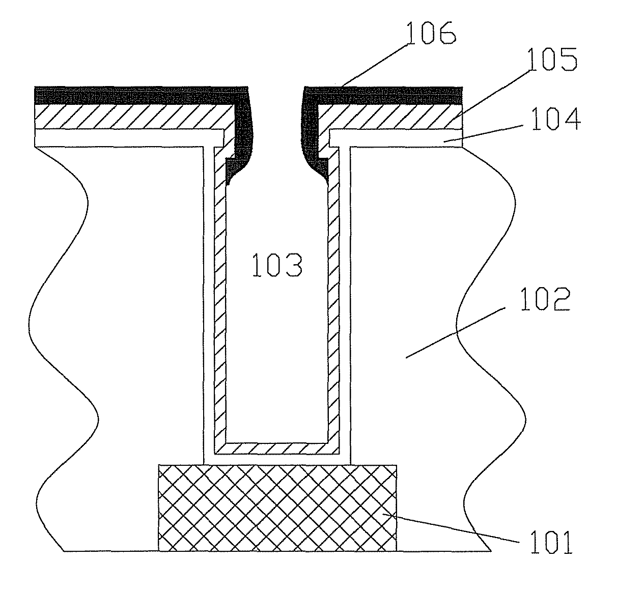
[0040]In step S1, a semiconductor substrate is provided. Referring to FIG. 6, the semiconductor substrate comprises at least an underlying metal interconnect layer 101 and an upper insulating dielectric layer 102 on top of the underlying metal interconnect layer 101, wherein the insulating dielectric layer 102 has a gap 103. Here, the wording of “underlying” only indicates the relative position to the upper metal interconnect layer, and does not represent a first metal interconnect layer. The semiconductor substrate further includes logical devices, power de...

embodiment 2

[0061]FIG. 13 is a schematic structural diagram of a method for filling a gap according to a second embodiment of the present invention. The method for filling a gap includes:

[0062]providing a semiconductor substrate, which at least has an underlying metal interconnect layer and an upper insulating dielectric layer on the underlying metal interconnect layer, the insulating dielectric layer having a gap;

[0063]forming a diffusion barrier layer and a seed layer sequentially in the gap and on a surface of the insulating dielectric layer outside the gap;

[0064]forming a mask layer on a surface of the seed layer outside the gap;

[0065]depositing a metal layer on the semiconductor substrate with the mask layer, and the metal layer being filled in the gap; and

[0066]performing a planarization process to remove the metal layer, the seed layer and the diffusion barrier layer outside the gap so as to form a metal interconnect layer.

[0067]The difference between the above steps in this embodiment a...


PUM

PropertyMeasurementUnit
thicknessaaaaaaaaaa
sizeaaaaaaaaaa
sizeaaaaaaaaaa

Abstract

A method for filling a gap includes: providing a semiconductor substrate, at least having an metal interconnect layer and an insulating dielectric layer on top of the underlying metal interconnect layer, the insulating dielectric layer having a gap; forming a diffusion bather layer and a seed layer sequentially in the gap and on a surface of the insulating dielectric layer outside the gap; forming a mask layer on a surface of the seed layer outside of the gap; and depositing a metal layer on the semiconductor substrate with the mask layer, the metal layer filling the gap.

Description

CROSS REFERENCE TO RELATED APPLICATIONS[0001]The present application claims the priority of Chinese Patent Application No. 201010590432.4, entitled “Method for Filling a Gap”, and filed on Dec. 15, 2010, the entire disclosure of which is incorporated herein by reference.BACKGROUND OF THE INVENTION[0002]1. Field of the Invention[0003]The present invention relates to semiconductor technology, and particularly relates to a method for filling a gap.[0004]2. Background of the Invention[0005]With the increasing requirement for the high integrity and high performance of Ultra Large Scale Integrated circuit, semiconductor technology is developing towards 22 nm technology node and even smaller critical size. However, the operation speed of chips is obviously influenced by Resistance Capacitance Delay Time (RC Delay Time) caused by metal lines. Thus, in current semiconductor manufacturing technology, copper metal interconnect with lower resistivity is adopted to substitute traditional aluminu...

Claims


Application Information

Patent Timeline
Patent Type & Authority Applications(United States)
IPC IPC(8): H01L21/768
CPCH01L23/53238H01L21/76898H01L21/76859H01L21/76873H01L2924/0002H01L21/76879H01L2924/00
Inventor ZHAO, CHAOWANG, WENWUZHONG, HUICAI
Owner INST OF MICROELECTRONICS CHINESE ACAD OF SCI
Why Eureka
Try Eureka