Semiconductor device, display device provided with same, and method for manufacturing semiconductor device

a semiconductor and display device technology, applied in static indicating devices, instruments, optics, etc., can solve the problems of increasing the manufacturing cost, the electro-optical layer, so as to prevent the failure of the first semiconductor element due to the breakage of the polycrystalline semiconductor layer, the effect of increasing the mobility of the channel layer and increasing the speed

Inactive Publication Date: 2012-08-09
SHARP KK
View PDF10 Cites 44 Cited by
  • Summary
  • Abstract
  • Description
  • Claims
  • Application Information

AI Technical Summary

Benefits of technology

[0056]In Aspect 1 of the present invention, in the first semiconductor element, a polycrystalline layer is formed to cover at least the surface elevation of the first structure, and the surface elevation of the first structure does not cause breakage of the polycrystalline semiconductor layer when the polycrystalline semiconductor layer is formed. As a result, failure of the first semiconductor element due to the breakage of the polycrystalline semiconductor layer can be prevented. On the other hand, in the second semiconductor element, because the thickness of the second structure is larger than the thickness of the first structure, the second structure can be used as the light-shielding layer or as a wiring with low wiring resistance.
[0057]In Aspect 2 of the present invention, because the surface elevation of the first structure has a tapered edge, the surface elevation of the first structure is less likely to cause breakage of the polycrystalline semiconductor layer. As a result, failure of the first semiconductor element due to the breakage of the polycrystalline semiconductor layer can be prevented even more effectively.
[0058]In Aspect 3 of the present invention, in the bottom gate type thin film transistor, the channel layer is formed of the polycrystalline semiconductor layer. As a result, the mobility of the channel layer increases, and therefore the bottom gate type thin film transistor can operate at a higher speed. Also, because the breakage of the polycrystalline silicon layer at the edge of the gate electrode can be prevented, the bottom gate type thin film transistor can operate reliably. In the light sensor, the light-shielding layer can block the light entering through a second surface of the insulating substrate, which is on the side opposite from the first surface of the insulating substrate on which the bottom gate type thin film transistor is formed. Therefore, if the light sensor is used as a touch sensor, the detection sensitivity of the light sensor can be increased.
[0059]According to Aspect 4 of the present invention, because the light-shielding layer is constituted only of the second layer that is made of the same material as the gate electrode, the light-shielding layer can easily be deposited. Also, because the second layer has a larger film thickness than the gate electrode, the light-shielding layer can block the light entering from the second surface side.
[0060]According to Aspect 5 of the present invention, because the light-shielding layer is composed of multiple layers including the second layer having the same film thickness as the gate electrode, the light entering from the second surface side can be blocked more effectively.
[0061]According to Aspect 6, because the channel layer of the bottom gate type thin film transistor is a polycrystalline semiconductor layer containing lateral crystals with large crystal grain diameters and having a direction of long axis that matches the direction of channel length, the mobility of the channel layer increases. As a result, the bottom gate type thin film transistor can operate at a higher speed.

Problems solved by technology

Thus, because the gate electrode of TFT is formed over the silicon layer and the light-shielding layer is formed below the silicon layer, the gate electrode and the light-shielding layer cannot be formed in the same process.
This makes the manufacturing process of liquid crystal panel complex and increases the manufacturing cost.

Method used


Image

  • Semiconductor device, display device provided with same, and method for manufacturing semiconductor device
  • Semiconductor device, display device provided with same, and method for manufacturing semiconductor device
  • Semiconductor device, display device provided with same, and method for manufacturing semiconductor device

Examples


modification examples

4. Modification Examples

4.1 Modification Example 1

[0130]When the amorphous silicon layer fully melts to form the polycrystalline silicon layer, to prevent the amorphous silicon layer from breaking over the edges of the gate electrode, the edges of the gate electrode may be tapered instead of making the film thickness of the gate electrode 110 small as in the case of the semiconductor device 100 shown in FIG. 5. FIG. 9 is a cross-sectional view showing the configuration of the semiconductor device 200 including the TFT 41 according to Modification Example 1 of the present invention, whose gate electrode 210 has tapered edges. Of the constituting elements of the semiconductor layer 200 shown in FIG. 9, those identical to the constituting elements of the semiconductor device 100 shown in FIG. 5 are provided with the same reference characters, and descriptions of those elements are omitted.

[0131]As shown in FIG. 9, the edges of the gate electrode 210 are tapered. The amorphous silicon l...

modification example 2

4.2 Modification Example 2

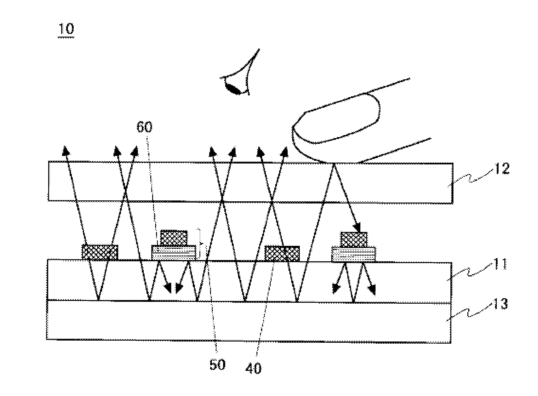
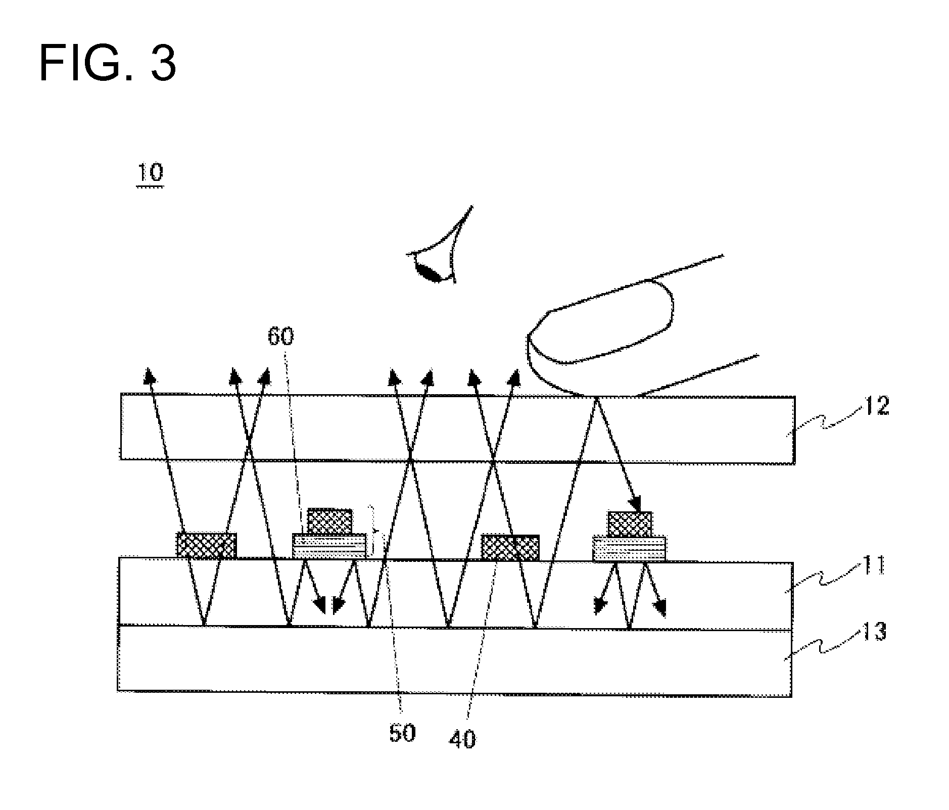
[0135]In the semiconductor device 100 shown in FIG. 4, the light-shielding layer 60 of the photodiode 50 is formed by patterning the multi-layered metal film in which the second metal layer 113 made of an alloy containing aluminum as a chief element is layered over the first metal layer 111 made of an alloy containing tungsten as a chief element. However, the light-shielding layer may also be formed by patterning a multi-layered metal film composed of three or more metal layers including a first metal layer 111 made of the same material and having the same film thickness as the gate electrode 110 of the TFT 40. In this case, because the film thickness of the light-shielding layer becomes larger, the light projected directly from backlight light source can be more effectively blocked from entering the photodiode, and therefore the light that is supposed to be detected, i.e., the light projected from the backlight light source and reflected by a finger or the...

modification example 3

4.3 Modification Example 3

[0138]In the semiconductor device 100 shown in FIG. 5, the gate electrode 110 of the TFT 40 is formed only on the glass substrate 101. However, instead of the TFT 40, a double gate type TFT, which has gate electrodes over and under the island-shaped silicon layer 120, may be formed. FIG. 10 is a cross-sectional view showing the configuration of the semiconductor device 300 according to Modification Example 3 of the present invention, in which a double gate type TFT 42 is included. Of the constituting elements of the semiconductor device 300 shown in FIG. 10, those identical to the constituting elements of the semiconductor device 100 shown in FIG. 5 are provided with the same reference characters, and descriptions of those elements are omitted.

[0139]As shown in FIG. 10, in the double gate type TFT 42, as in the case of the TFT 40 of the semiconductor device 100 shown in FIG. 5, not only a first gate electrode 410 is formed on the glass substrate 101, but al...


PUM


Abstract

Disclosed is a semiconductor device including plural types of semiconductor elements having structures that have respective thicknesses suitable for their uses formed in the same process. A semiconductor device (100) includes a TFT (40) and a photodiode (50). A gate electrode (110) of the TFT (40) and a light-shielding layer (60) of the photodiode (50) are formed in the same process. However, because the film thickness of the gate electrode (110) is small, the breakage of an island-shaped silicon layer (120), which will be the channel layer, at the edge of the gate electrode (110) can be prevented. Also, because the film thickness of the light-shielding layer (60) is large, the light entering through a surface of a glass substrate (101) on the side opposite from the surface on which the TFT is formed can be reliably blocked by the light-shielding layer (60). Consequently, the detection sensitivity of the photodiode (50) can be increased.

Description

TECHNICAL FIELD[0001]The present invention relates to a semiconductor device, a display device equipped with the semiconductor device, and a method for manufacturing the semiconductor device. More particularly, the present invention relates to a semiconductor device in which multiple types of semiconductor elements are formed on the same insulating substrate, a display device equipped with the semiconductor device, and a method for manufacturing the semiconductor device.BACKGROUND ART[0002]In recent years, development of active matrix type liquid crystal display devices including a liquid crystal panel having a touch-panel feature has been underway. For such liquid crystal panels of liquid crystal display devices, in each of the pixel formation sections formed in the display region where images are displayed, a thin film transistor (hereinafter referred to as “TFT”) that functions as a switching element and a photodiode that functions as a touch sensor are provided. Also, in the fra...

Claims


Application Information

Patent Timeline
Patent Type & Authority Applications(United States)
IPC IPC(8): G06F3/038H01L21/20H01L29/786
CPCH01L27/1214H01L27/14623H01L27/14632G02F2202/104G02F1/13338G02F1/136209G02F1/1368H01L29/78633
Inventor MIYAMOTO, TADAYOSHITOMIYASU, KAZUHIDEKATOH, SUMIO
Owner SHARP KK
Why Eureka
Try Eureka