Programmable LSI

a programmable lsi and programmable lsi technology, applied in logic circuits, digital storage, instruments, etc., can solve the problems of increasing the power consumption affecting the performance of the programmable lsi, so as to reduce the frequency of refresh operation and reduce power consumption. , the effect of reducing the configuration tim

Inactive Publication Date: 2012-08-23
SEMICON ENERGY LAB CO LTD
View PDF2 Cites 64 Cited by
  • Summary
  • Abstract
  • Description
  • Claims
  • Application Information

AI Technical Summary

Benefits of technology

[0062]The memory element includes a storage element whose predetermined node is set in a floating state when a transistor whose channel is formed in an oxide semiconductor layer is turned off and holds a signal potential corresponding to data in the node. The off-state current of the transistor whose channel is formed in the oxide semiconductor layer is extremely low. Thus, a fluctuation in the signal potential due to leakage of the transistor can be inhibited. In this manner, each storage element included in the memory element can continue to hold a signal potential corresponding to data (configuration data) for a long time after supply of power supply voltage to the memory element is stopped. In short, the memory element can function like a nonvolatile m

Problems solved by technology

Thus, the power consumption of the programmable LSI is increased.
Further, since the DRAM is a volatile memory, it is necessary to store data in the DRAM every time supply of power supply voltage to the programmable LSI is started.
Further, large-scale data transfer from

Method used


Image

  • Programmable LSI
  • Programmable LSI
  • Programmable LSI

Examples


embodiment 1

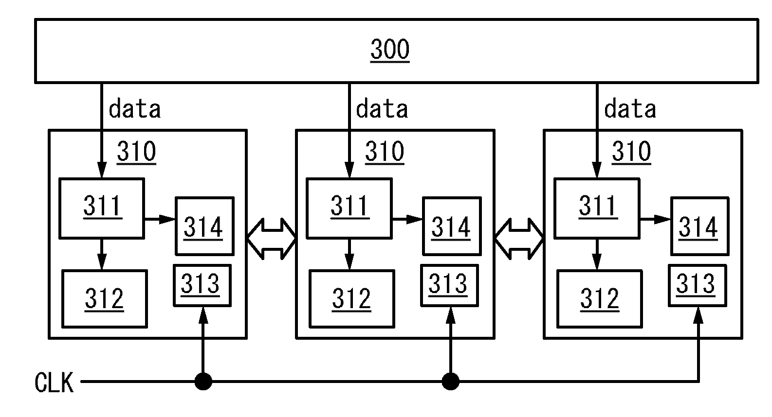
[0092]One aspect of a programmable LSI is described.

[0093]FIG. 1A schematically illustrates the structure of a programmable LSI. The programmable LSI includes a plurality of logic elements 310 and a memory element 300. FIG. 1A typically illustrates the three logic elements 310. The number of logic elements can be a given number. Alternatively, the programmable LSI may further include plural sets of the plurality of logic elements 310 and the memory element 300. Alternatively, the programmable LSI may further include a multiplier, a RAM block, a PLL block, or an I / O element. The multiplier has a function of multiplying plural pieces of data at high speed. The RAM block has a function of storing given data as a memory. The PLL block has a function of supplying a clock signal to a circuit in the programmable LSI. The I / O element has a function of controlling signal passing between the programmable LSI and an external circuit.

[0094]The logic element 310 includes a configuration memory 3...

embodiment 2

[0141]In this embodiment, a more specific aspect of the memory element 300 in Embodiment 1 is described.

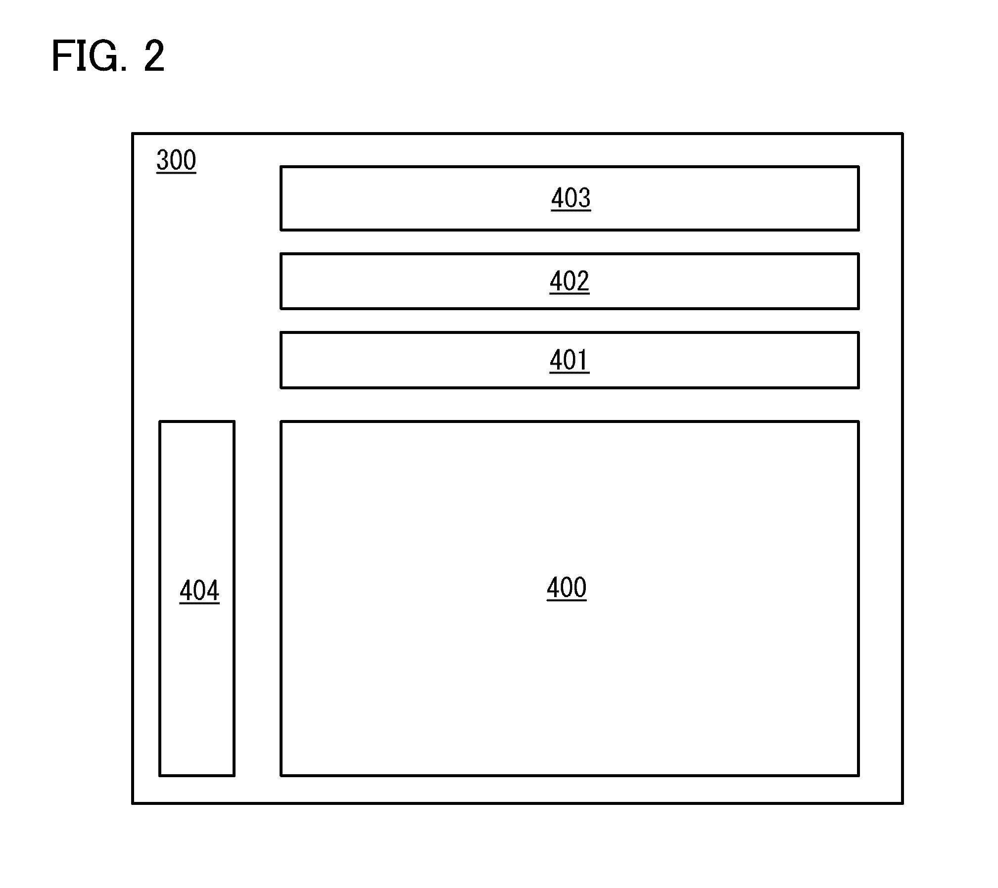
[0142]The memory element 300 can include a memory cell array including the plurality of storage elements in Embodiment 1 (having Structure 1 of the storage element, Structure 2 of the storage element, or Structure 3 of the storage element) arranged in matrix.

[0143]The memory element 300 can include any of or all of a decoder (a row decoder or a column decoder), a precharge circuit, a sense amplifier, and a temporary storage circuit in addition to the memory cell array. Note that some of these circuits can be merged into a single circuit. For example, the sense amplifier may function as a temporary storage circuit.

[0144]The decoder (the row decoder or the column decoder) has a function of selecting a given storage element in the memory cell array. The memory element 300 writes and reads data to and from the storage element selected by the decoder (the row decoder or the column deco...

embodiment 3

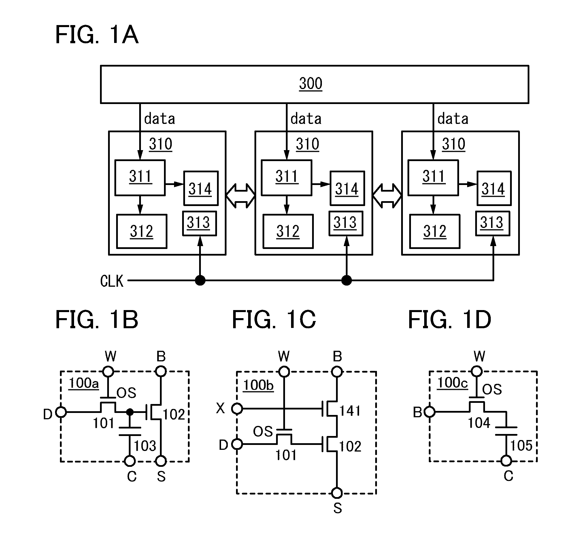
[0202]In this embodiment, one aspect of the configuration memory 311 included in the logic element 310 is described. The configuration memory 311 can be formed using, for example, a latch circuit or a capacitor.

[0203]FIGS. 10A and 10B each illustrate an example in which a storage element 501 or a storage element 502 includes a latch circuit as the storage element included in the configuration memory 311. The latch circuit can be formed using an inverter 511 and an inverter 512. Data input from an input terminal IN is retained in the storage element 501 and the storage element 502, and is output from an output terminal OUT.

[0204]In the case where the configuration memory 311 is formed using the storage element 501 or the storage element 502, the configuration memory 311 can be used as the sense amplifier 401 or part of the sense amplifier 401. In other words, the structure of the configuration memory 311 and the structure of the sense amplifier 401 can be used in common partly or ent...


PUM


Abstract

A low-power programmable LSI that can perform configuration (dynamic configuration) at high speed and can quickly start is provided. The programmable LSI includes a plurality of logic elements and a memory element for storing configuration data to be input to the plurality of logic elements. The plurality of logic elements each include a configuration memory. Each of the plurality of logic elements performs different arithmetic processing and changes an electrical connection between the logic elements in accordance with the configuration data stored in the configuration memory. The memory element is formed using a storage element including a transistor whose channel is formed in an oxide semiconductor layer and a node set in a floating state when the transistor is turned off.

Description

BACKGROUND OF THE INVENTION[0001]1. Field of the Invention[0002]The present invention relates to semiconductor devices. In particular, the present invention relates to programmable LSIs and semiconductor devices including the programmable LSIs. Further, the present invention relates to electronic devices including the semiconductor devices.[0003]2. Description of the Related Art[0004]Programmable LSIs show flexibility in a reduction in development period and a change in design specification as compared to conventional application specific integrated circuits (ASIC) and gate arrays, which is advantageous. Programmable LSIs are widely used in semiconductor devices.[0005]A programmable LSI includes, for example, a plurality of logic elements and wirings between the logic elements. When the functions of the logic elements are changed, the function of the programmable LSI can be changed. The logic element is formed using, for example, a look-up table or the like. The look-up table perfor...

Claims


Application Information

Patent Timeline
IPC IPC(8): G11C11/24G11C7/00
CPCH03K19/1778G11C7/1006G11C11/405G11C5/06G11C11/401G11C11/4072G11C7/00
Inventor KUROKAWA, YOSHIYUKI
Owner SEMICON ENERGY LAB CO LTD
Why Eureka
Try Eureka