Organic el display

Inactive Publication Date: 2012-09-13
UNIFIED INNOVATIVE TECH
View PDF3 Cites 79 Cited by
  • Summary
  • Abstract
  • Description
  • Claims
  • Application Information

AI Technical Summary

Benefits of technology

[0020]The organic EL display of the present invention can achieve significant improvement of color conversion efficiency. This working effect arises from the facts that (a) in the present invention, formation of the color conversion layer on the barrier layer of the organic EL element substrate to discreate a distance between the barrier layer and the color conversion layer corresponds to making all of light exited from the barrier layer reach a surface of the color conversion layer of an intended sub pixel in the conventional structure, and that (b) the absence of a low refractive index layer between the barrier layer and the color conversion layer, i.e., in a path from the light emitting layer to the color conversion layer reduces reflection losses at interfaces between the respective layers.
[0021]Also, in the organic EL display of the present invention, growth of a defect referred to as a dark area or dark spot is hardly recognized. It is thought that this effect arises from the fact that the separation wall is formed before the formation of the organic EL layer in the present invention, which is distinct from the conventional organic EL element substrate in which the separation wall is formed after the formation of the organic EL layer. This is because formation of the separation wall before forming the organic EL layer make it possible to sufficiently carry out a heating process as countermeasures against outgas from the separation wall. Further, another factor of this effect is that the organic EL layer is divided into the plurality of parts in the organic EL display of the present invention. Thereby, the defect referred to as the dark area or dark spot does not propagate throughout the dis

Problems solved by technology

If the bonding gap is too wide, a crosstalk problem that light penetrates into an adjacent pixel is concerned.
In particular, in the case of enclosing the filler in the bonding gap, if the bonding gap is too narrow, the included filler may distribute unevenly.
In addition, in the case where the transversely deviated light enters an adjacent different color sub pixel, the color conversion layer of the adjacent sub pixel may emit converted light and the emitted light may produce undesired hue.
Further, the thin-film organic EL layer has extremely low mechanical strength.
Therefore in the organic EL display employing the bonding structure as described above, mechanical bonding strength in the display area can not be expected at all.
Also, a structure involving a hollow bonding gap has been proposed by many institutions from the start time of the organic EL display; however, it goes without saying that such a structure is not advantageous to manufacturing of the large screen display.
However, in the case where the structure in which the filler is enclosed in the bonding gap is adopted and the filler has a lower refractive index than that of the barrier layer, total reflection occurs at an interface between the barrier layer and the filler, preventing sufficient amount of light from being transmitted, and therefore resulting in an optical loss.
In addition, such filler is a special and expensive material, and therefore becomes a factor for increasing manufacturing cost.
Further, Japanese Patent Laid-Open No. 2006-32010 does not disclose sealing based on substrate bonding; however, the sealing is practically required.
Therefore, as described above, there is a concern on insuffi

Method used


Image

  • Organic el display
  • Organic el display
  • Organic el display

Examples


example 1

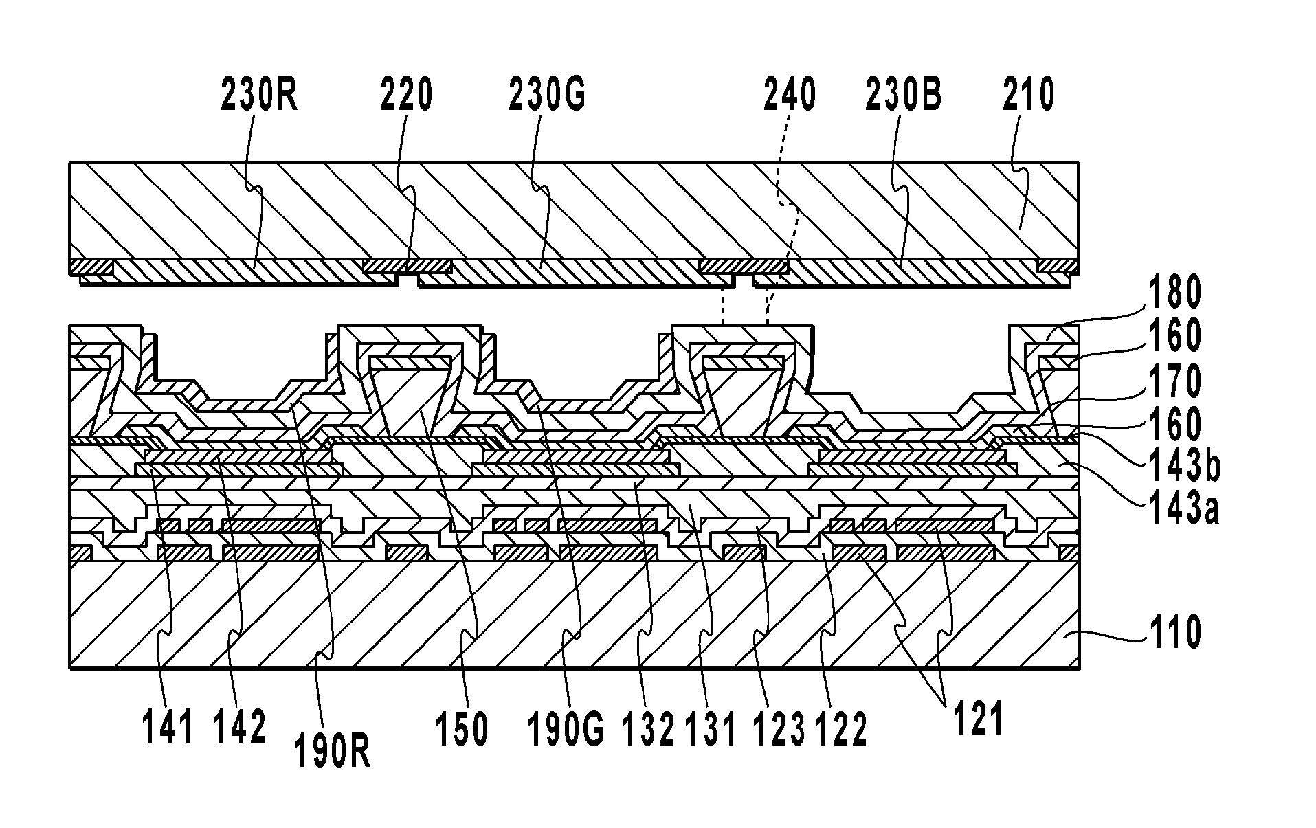
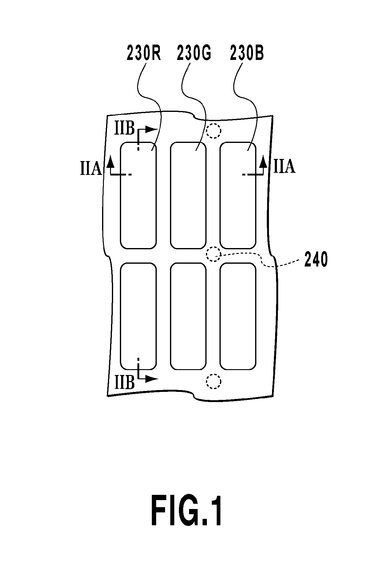
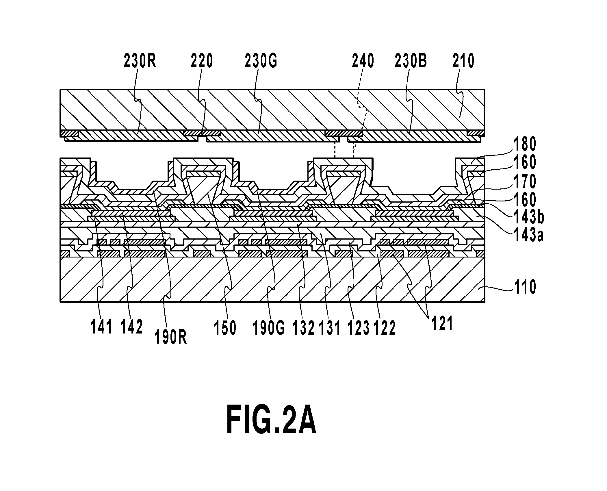
[0067]The present example is an example of the organic EL display of the first embodiment of the present invention. An organic EL display in the present example has a nominal size of 3 inches, and each pixel has a size of 60 μm×180 μm×RGB. Also, a color filter substrate was used, in which the black matrix 220 and three types of color filters 230 were formed on the sealing substrate 210.

[0068]On alkali-free glass having a size of 200 mm×200 mm×0.7 mm (manufactured by Asahi glass, AN-100), the electrically conductive layer 121 (including switching elements and wiring), insulating layer 122, and protective layer 123 for a plurality of display parts were formed. Then, the planarizing layer 131 was formed on the protective layer 123. The planarizing layer 131 was patterned to form a contact hole for connecting the electrically conductive layer 121 with the reflective electrode 142 in each of the sub pixels (light emitting parts) by a photolithography method, wherein the contact hole had ...

example 2

[0086]The present example is another example of the organic EL display of the, first embodiment of the present invention. An organic EL display in the present example has a nominal size of 3 inches, and each pixel has a size of 60 μm×180 μm×RGB. Also, a color filter substrate, in which the black matrix 220 and three types of color filters 230 were formed on the sealing substrate 210, was used.

[0087]First, in the same procedure as that in Example 1, the layers including and below the inorganic passivation layer 132 were formed.

[0088]Then, the separation wall 150 made of Cu was formed by a Cu plating method. The separation wall 150 was constituted of the plurality of striped parts extending longitudinally and the plurality of striped parts extending transversely. The separation wall 150 had the openings in the locations corresponding to the respective light emitting parts. Further, each of the striped parts constituting the separation wall 150 had a rectangular cross-sectional shape h...

example 3

[0092]The present example is an example of the organic EL display of the second embodiment of the present invention. An organic EL display in the present example has a nominal size of 6 inches, and each pixel has a size of 100 μm×300 μm×RGB. Also, a color filter substrate was used, in which the black matrix 220 and three types of color filters 230 were formed on the sealing substrate 210.

[0093]First, in the same procedure as that in Example 1 except that the size of each pixel was changed, the layers including and below the inorganic passivation layer 132 were formed. Subsequently, an IZO film was formed by a sputtering method and patterned in the same procedure as that in Example 1, to form the underlying layer 141 constituted of the plurality of parts separated for each of the sub pixels, and the underlying layer 144 for auxiliary wiring constituted of the plurality of striped parts having a width of 16 μm in gaps between transversely adjacent sub pixels. Each of the striped parts...


PUM


Abstract

An object of the present invention is to provide an organic EL display that has a reduced optical loss and high efficiency, and can be manufactured by an inexpensive method. The organic EL display of the present invention is formed by bonding an organic EL element substrate including a substrate, reflective electrode, organic EL layer, separation wall, barrier layer, transparent electrode, and color conversion layer; and a sealing substrate together, wherein: the reflective electrode includes a plurality of partial electrodes; the organic EL layer is formed on the reflective electrode and includes a plurality of parts separated by the separation wall; the transparent electrode is formed on the organic EL layer; the barrier layer covers the separation wall and the transparent electrode, and has a recessed part in a location corresponding to the reflective electrode; and the color conversion layer is formed in the recessed part.

Description

REFERENCE TO RELATED APPLICATIONS[0001]This application is a national stage application under 35 USC 371 of International Application No. PCT / JP2009 / 006171, filed Nov. 17, 2009, the entire contents of which are incorporated herein by reference.FIELD OF THE INVENTION[0002]The present invention mainly relates to an organic EL display.BACKGROUND OF THE INVENTION[0003]A panel unit of an organic EL display having a top emission structure typically has a configuration in which an organic EL element substrate (a TFT substrate) and a color filter substrate are bonded together.[0004]An organic EL element substrate having a conventional structure includes, for example, a glass substrate, a TFT structure, planarizing resin, an inorganic passivation film that may be optionally provided, an underlying layer for enhancing adhesiveness, reflective electrodes, an insulating film that has openings in locations serving as light emitting parts, an organic EL layer, a transparent electrode (including s...

Claims


Application Information

Patent Timeline
IPC IPC(8): H01L27/32
CPCH01L27/322H01L27/3246H01L2251/5315H01L51/5203H01L51/5228H01L51/0005H10K59/38H10K71/135H10K59/122H10K50/805H10K50/822H10K50/824H10K50/828H10K50/8428H10K2102/3026H10K50/818H10K50/844
Inventor NAKAMURA, HIDEYO
Owner UNIFIED INNOVATIVE TECH
Why Eureka
Try Eureka