Method for producing semiconductor device and semiconductor device

a technology of semiconductor devices and semiconductor devices, applied in semiconductor devices, diodes, electrical devices, etc., can solve problems such as the difference in high-speed operation properties, and achieve the effect of high degree of integration and high-speed operation

Active Publication Date: 2012-09-13
UNISANTIS ELECTRONICS SINGAPORE PTE LTD
View PDF6 Cites 8 Cited by
  • Summary
  • Abstract
  • Description
  • Claims
  • Application Information

AI Technical Summary

Benefits of technology

[0106]The present invention can provide a semiconductor device in whic

Problems solved by technology

Thus, the solid-state imaging device illustrated in FIG. 17 has a problem that it is inferior in a high-speed operation property to a s

Method used


Image

  • Method for producing semiconductor device and semiconductor device
  • Method for producing semiconductor device and semiconductor device
  • Method for producing semiconductor device and semiconductor device

Examples


first embodiment

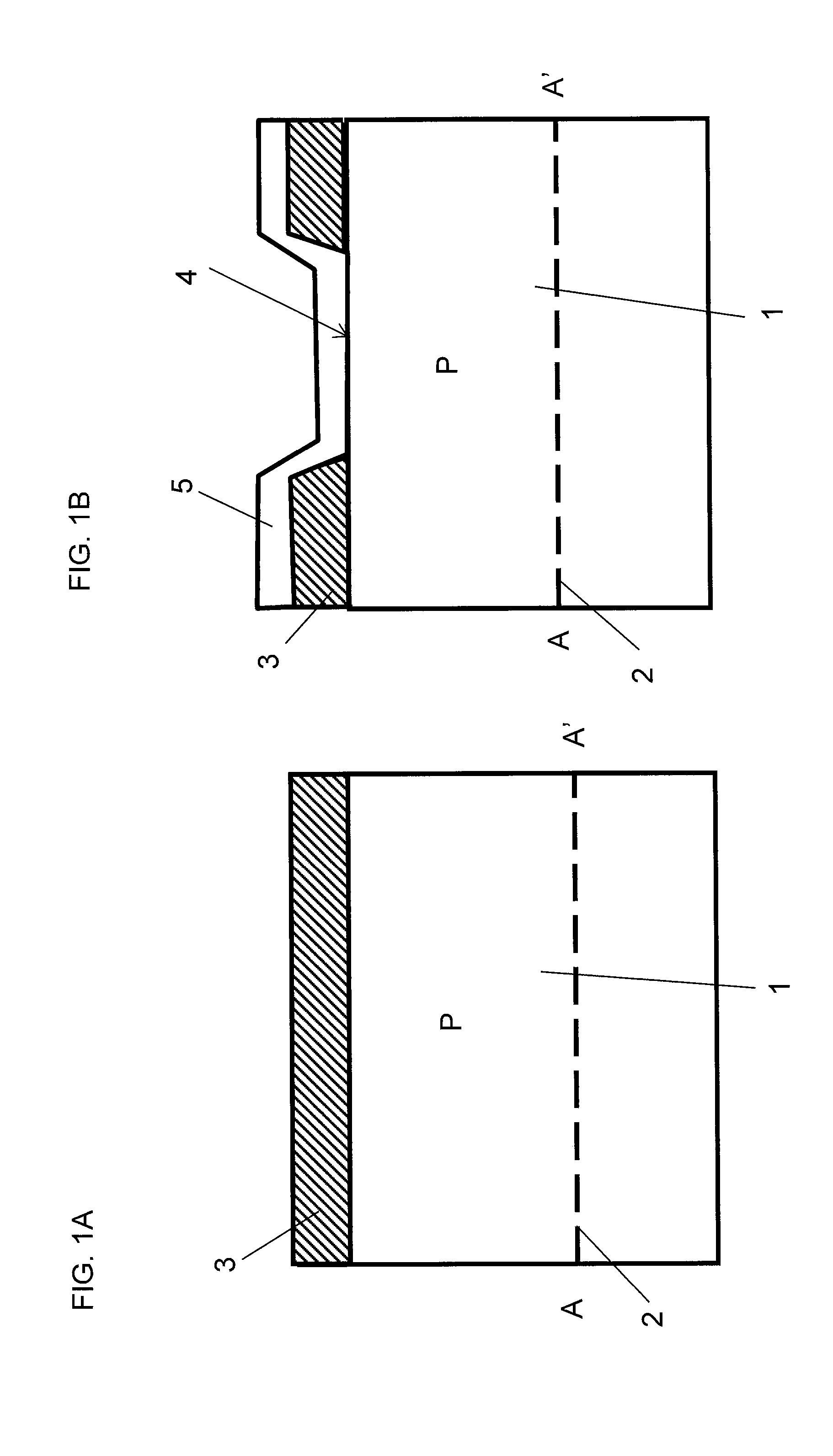
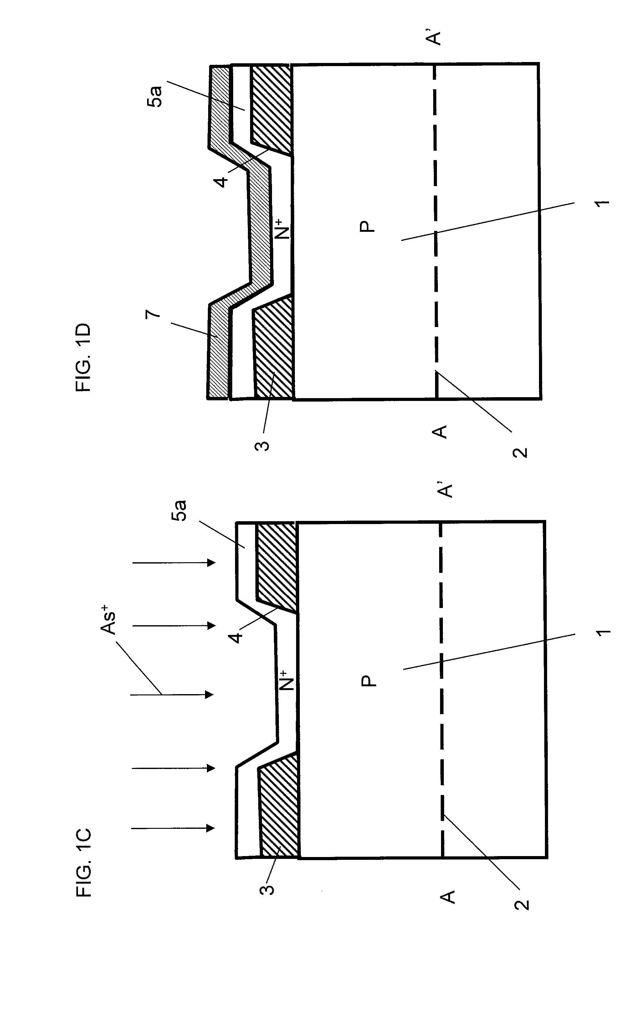
[0157]FIGS. 1A to 1L illustrate a method for producing a solid-state imaging device according to a first embodiment of the present invention.

[0158]In the method for producing a solid-state imaging device according to this embodiment, as illustrated in FIG. 1A, a division layer 2 for dividing a first semiconductor substrate 1 into two portions of an upper portion and a lower portion is formed by doping the first semiconductor substrate 1 composed of P-type silicon with protons (H+) at a high concentration to a predetermined depth of the first semiconductor substrate 1 (refer to M. Bruel: “Silicon on Insulator material technology”, Electronics Letters Vol. 31, No. 14, pp. 1201-1202 (6 Jul., 1995)). A first silicon oxide layer 3, which is an insulating film, is formed on the first semiconductor substrate 1 by thermal oxidation or a CVD (chemical vapor deposition) process. Instead of the P-type silicon, the first semiconductor substrate 1 may be composed of an intrinsic semiconductor (i...

second embodiment

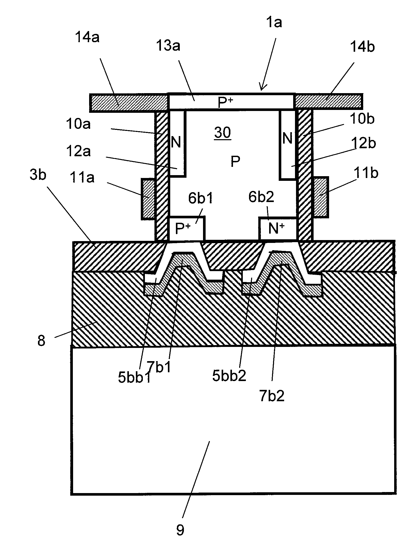
[0190]Hereinafter, a method for producing a semiconductor device including an SGT (surrounding gate transistor) according to a second embodiment of the present invention will be described with reference toFIG. 2.

[0191]In this embodiment, in the steps illustrated in FIGS. 1A to 1J out of the steps of the first embodiment illustrated in FIGS. 1A to 1L, the N+ polycrystalline silicon layer 5a constituting the signal line in FIG. 1J is replaced by an N+ polycrystalline silicon layer 55a that functions as a drain in an SGT. As in the first embodiment (refer to FIG. 1J), the metal layer 7 is bonded to the N+ polycrystalline silicon layer 55a; the N+ diffusion layer 6a is formed in the silicon pillar 1a by thermal diffusion of a donor impurity from the N+ polycrystalline silicon layer 55a.

[0192]In the embodiment, the step in FIG. 1J is followed by a step illustrated in FIG. 2. In this step, gate insulating layers 15a and 15b are formed in outer peripheral portions of the silicon pillar 1a...

third embodiment

[0197]Hereinafter, a method for producing a semiconductor device including SGTs according to a third embodiment of the present invention will be described with reference to FIGS. 3A and 3B. In this embodiment, an N-channel SGT and a P-channel SGT are formed on the same semiconductor substrate. The steps for producing the semiconductor device in the embodiment and a modification of the embodiment are the same as in the first embodiment unless otherwise specified below.

[0198]In the embodiment, referring to FIGS. 3A and 3B, an N-channel SGT is formed in an N-channel-SGT-forming region 1n and a P-channel SGT is formed in a P-channel-SGT-forming region 1p on the first semiconductor substrate 1.

[0199]The N-channel SGT in the N-channel-SGT-forming region 1n is formed in the same manner as the steps illustrated in FIGS. 1A to 1J of the first embodiment and the step illustrated in FIG. 2 of the second embodiment.

[0200]The P-channel SGT in the P-channel-SGT-forming region 1p is basically form...


PUM


Abstract

A method for producing a semiconductor device includes a step of forming a conductor layer and a first semiconductor layer containing a donor impurity or an acceptor impurity on a first semiconductor substrate; a step of forming a second insulating layer so as to cover the first semiconductor layer; a step of thinning the first semiconductor substrate to a predetermined thickness; a step of forming, from the first semiconductor substrate, a pillar-shaped semiconductor having a pillar-shaped structure on the first semiconductor layer; a step of forming a first semiconductor region in the pillar-shaped semiconductor by diffusing the impurity from the first semiconductor layer; and a step of forming a pixel of a solid-state imaging device with the pillar-shaped semiconductor into which the impurity has been diffused.

Description

RELATED APPLICATIONS[0001]Pursuant to 35 U.S.C. §119(e), this application claims the benefit of the filing date of Provisional U.S. Patent Application Ser. No. 61 / 450,335 filed on Mar. 8, 2011. The entire content of this application is hereby incorporated by reference.BACKGROUND OF THE INVENTION[0002]1. Field of the Invention[0003]The present invention relates to a method for producing a semiconductor device and a semiconductor device and, in particular, to a method for producing a semiconductor device including a transistor in which a channel region is formed in a semiconductor having a pillar-shaped structure, and the semiconductor device.[0004]2. Description of the Related Art[0005]Solid-state imaging devices such as CCDs and CMOS devices are widely used for video cameras, still cameras, and the like. Improvements in the performances of solid-state imaging devices such as a higher resolution, a higher operation speed, and a higher sensitivity have been demanded.[0006]As illustrat...

Claims


Application Information

Patent Timeline
IPC IPC(8): H01L27/06H01L21/8234H01L21/336H01L29/78H01L29/06
CPCH01L21/823487H01L29/8613H01L27/0629H01L27/088H01L27/092H01L27/14612H01L27/14632H01L27/14643H01L27/14687H01L27/14689H01L29/6609H01L29/66666H01L29/66909H01L29/7827H01L29/8083H01L21/823885
Inventor MASUOKA, FUJIOHARADA, NOZOMU
Owner UNISANTIS ELECTRONICS SINGAPORE PTE LTD
Why Eureka
Try Eureka