

Laser annealing apparatus and laser annealing method
a laser annealing and laser technology, applied in laser beam welding apparatus, transistors, manufacturing tools, etc., can solve the problem that the current laser cannot sufficiently perform activation, and achieve the effect of reducing the energy density necessary for activation, reducing the thermal load of pulse lasers, and reducing the heat capacity
- Summary
- Abstract
- Description
- Claims
- Application Information
AI Technical Summary
Benefits of technology
Problems solved by technology
Method used
Image

Examples
example 1
[0091]An example of the present invention will be then described.
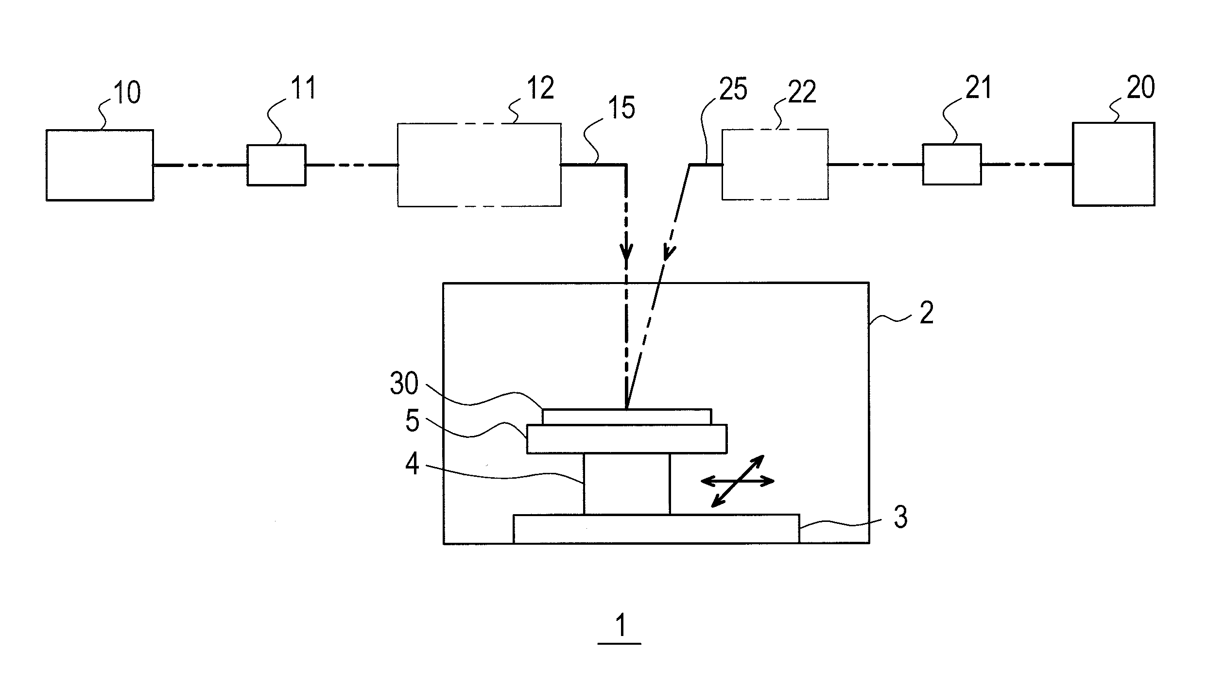
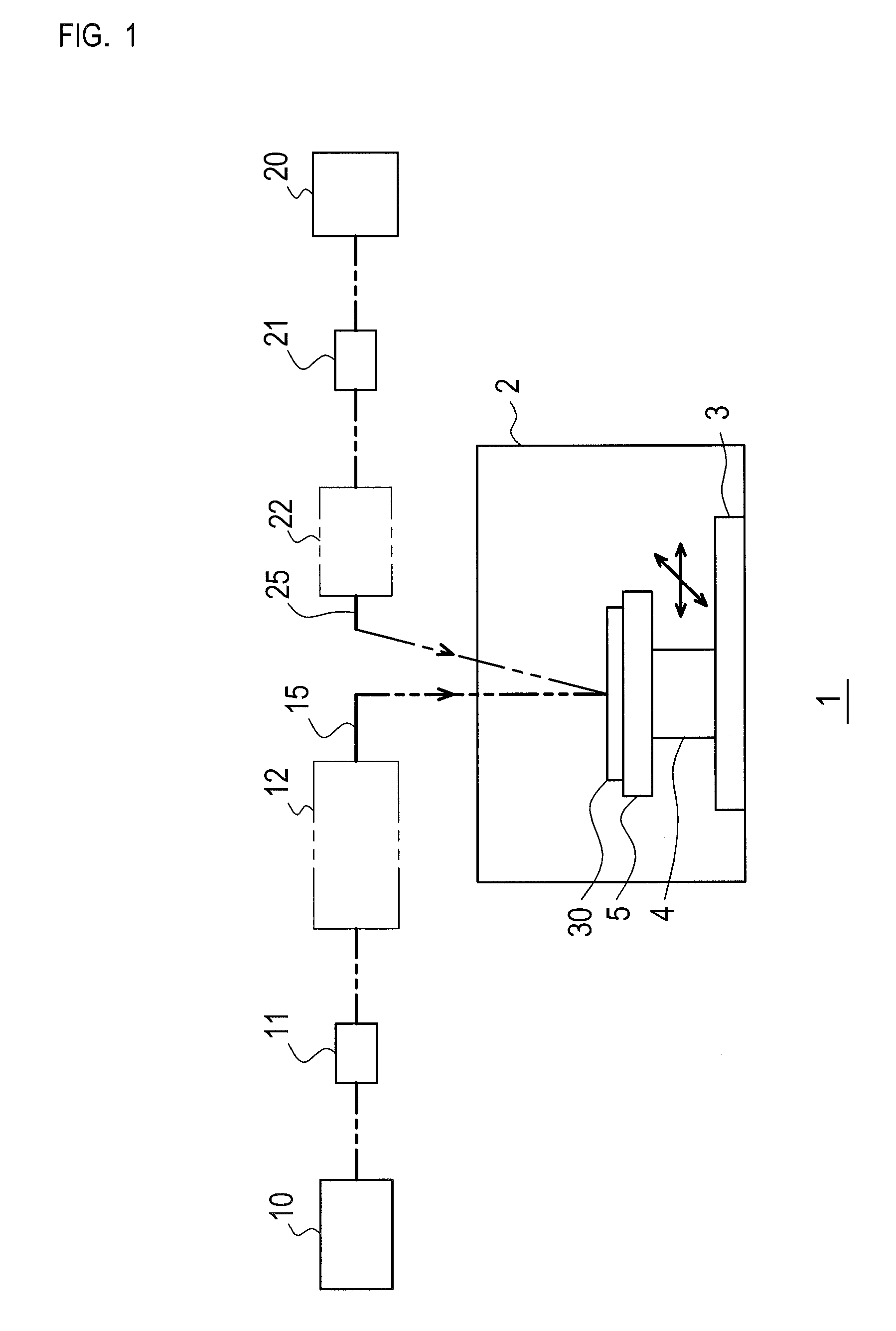
[0092]As the green pulse laser, second harmonics of LD-excited solid state laser (DPSS) were used, and as the pulse oscillation laser source, LD-excited Yb:YAG was used. A pulse laser beam (wavelength 515 nm) being output from the laser source and emitted to a semiconductor substrate was set to have a pulse width of 1200 ns, a rise time of 308 ns, a fall time of 92 ns, an energy density of 8 J / cm2, and a pulse frequency of 10 kHz, and the substrate was repeatedly overlap-irradiated therewith from directly above.
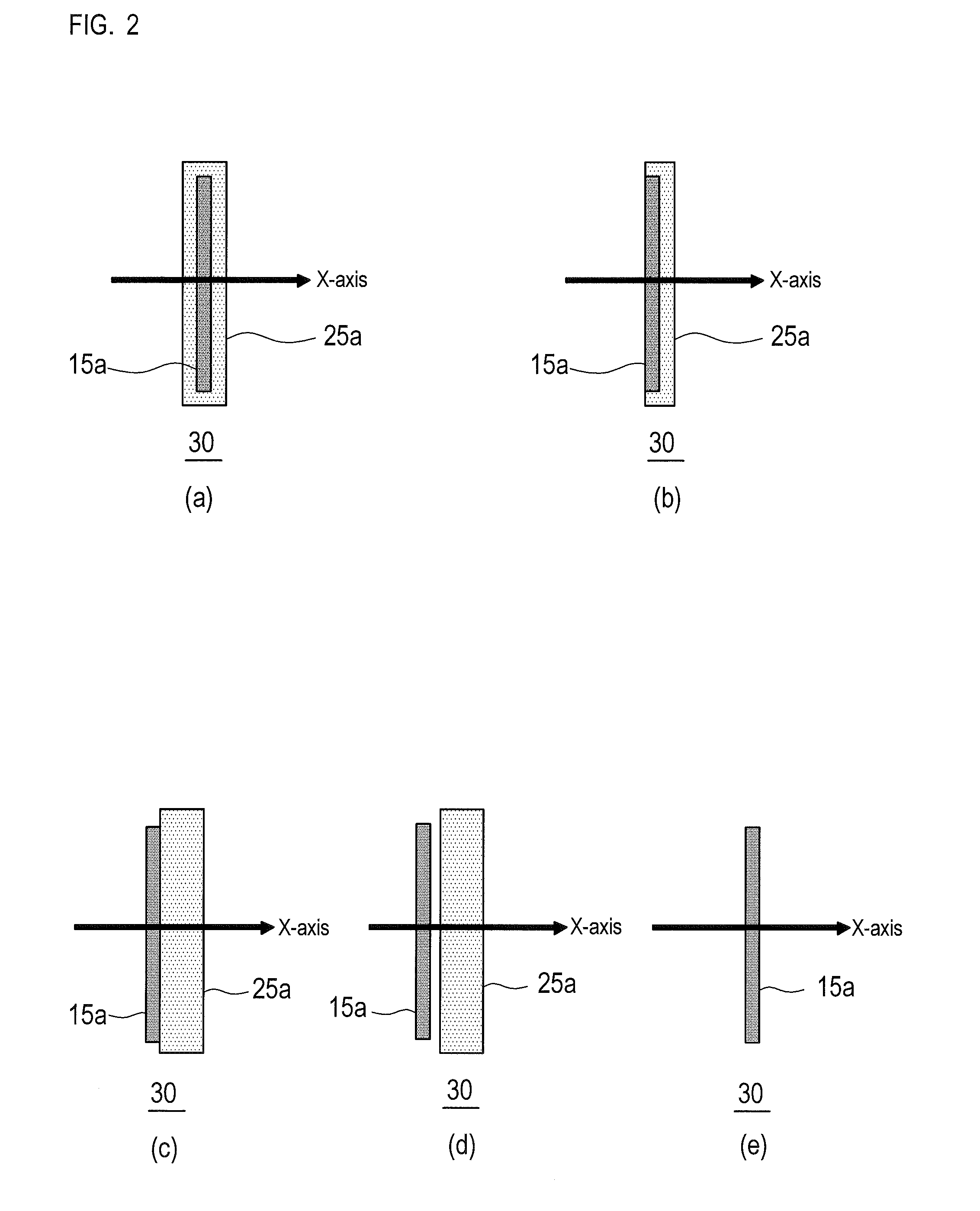
[0093]On the other hand, the substrate was continuously irradiated with a near-infrared laser beam having a wavelength of 808 nm, which was generated by a continuous wave laser source, in a power density of 11.3 kW / cm2.sec and at an angle of 45° to the substrate. These beams were emitted to the semiconductor substrate around at the same time, and shaped respectively by optical systems so that the size (short axi...
PUM
| Property | Measurement | Unit |
|---|---|---|
| temperature | aaaaa | aaaaa |
| activation depth | aaaaa | aaaaa |
| infrared wavelength | aaaaa | aaaaa |
Abstract
Description
Claims
Application Information