

Oxide semiconductor film and semiconductor device
a semiconductor film and amorphous oxide technology, applied in the direction of semiconductor devices, basic electric elements, electrical equipment, etc., can solve the problems of reducing and the reliability of amorphous oxide semiconductor films containing indium and zinc is reduced, so as to achieve stable electric characteristics, high reliability of semiconductors, and stable electric characteristics
- Summary
- Abstract
- Description
- Claims
- Application Information
AI Technical Summary
Benefits of technology
Problems solved by technology
Method used
Image

Examples
embodiment 1
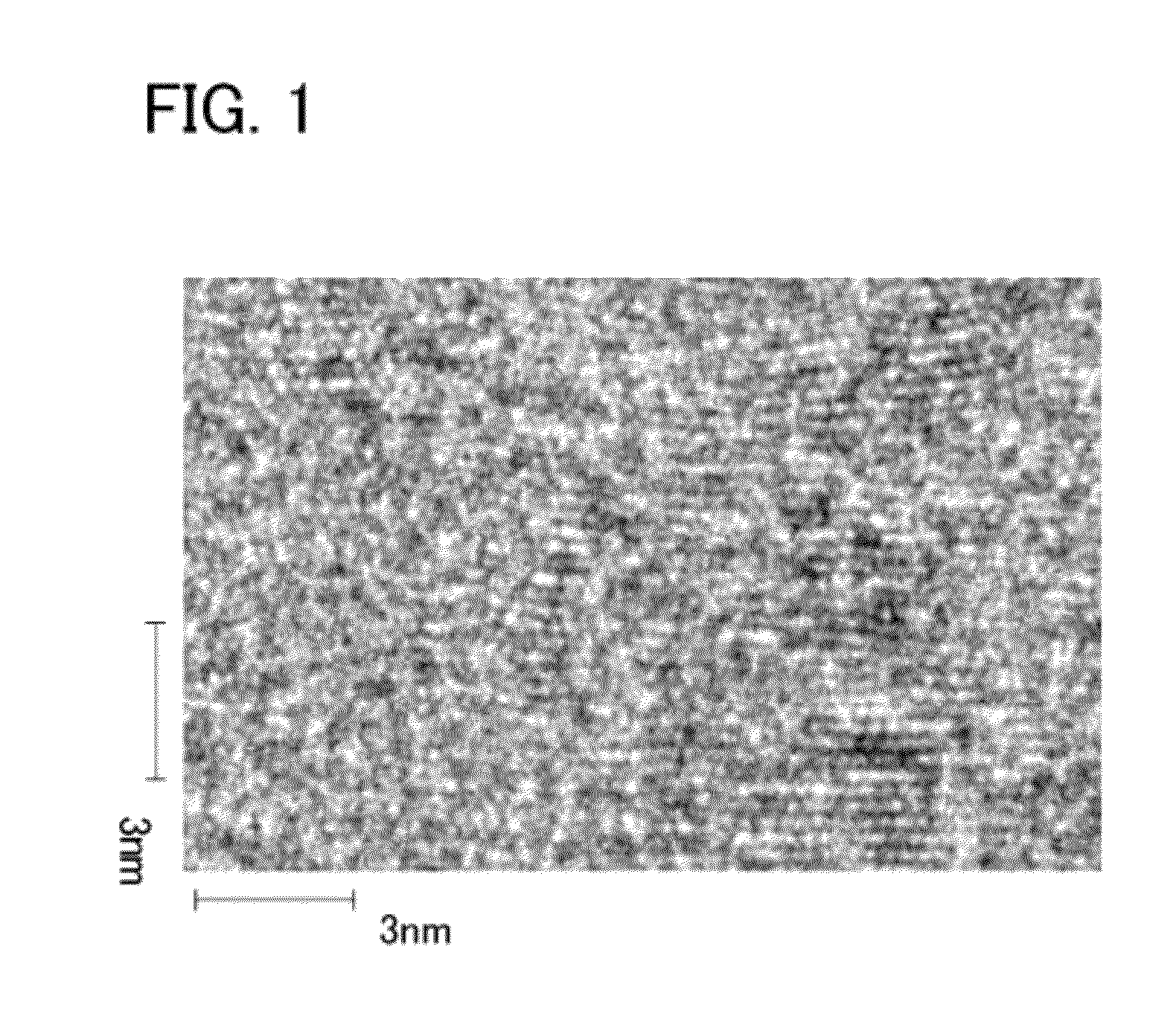
[0035]This embodiment shows a structure of an oxide semiconductor film essentially consisting of indium zinc oxide (hereinafter referred to as indium zinc oxide film) with reference to FIG. 1, FIGS. 2A and 2B, FIGS. 3A and 3B, and FIGS. 4A and 4B.
[0036]The indium zinc oxide film according to this embodiment includes a region having crystal structures. The region having crystal structures has a hexagonal crystal structure in which the a-b plane is substantially parallel to a surface of the indium zinc oxide film and a rhombohedral crystal structure in which the a-b plane is substantially parallel to the surface of the indium zinc oxide film.
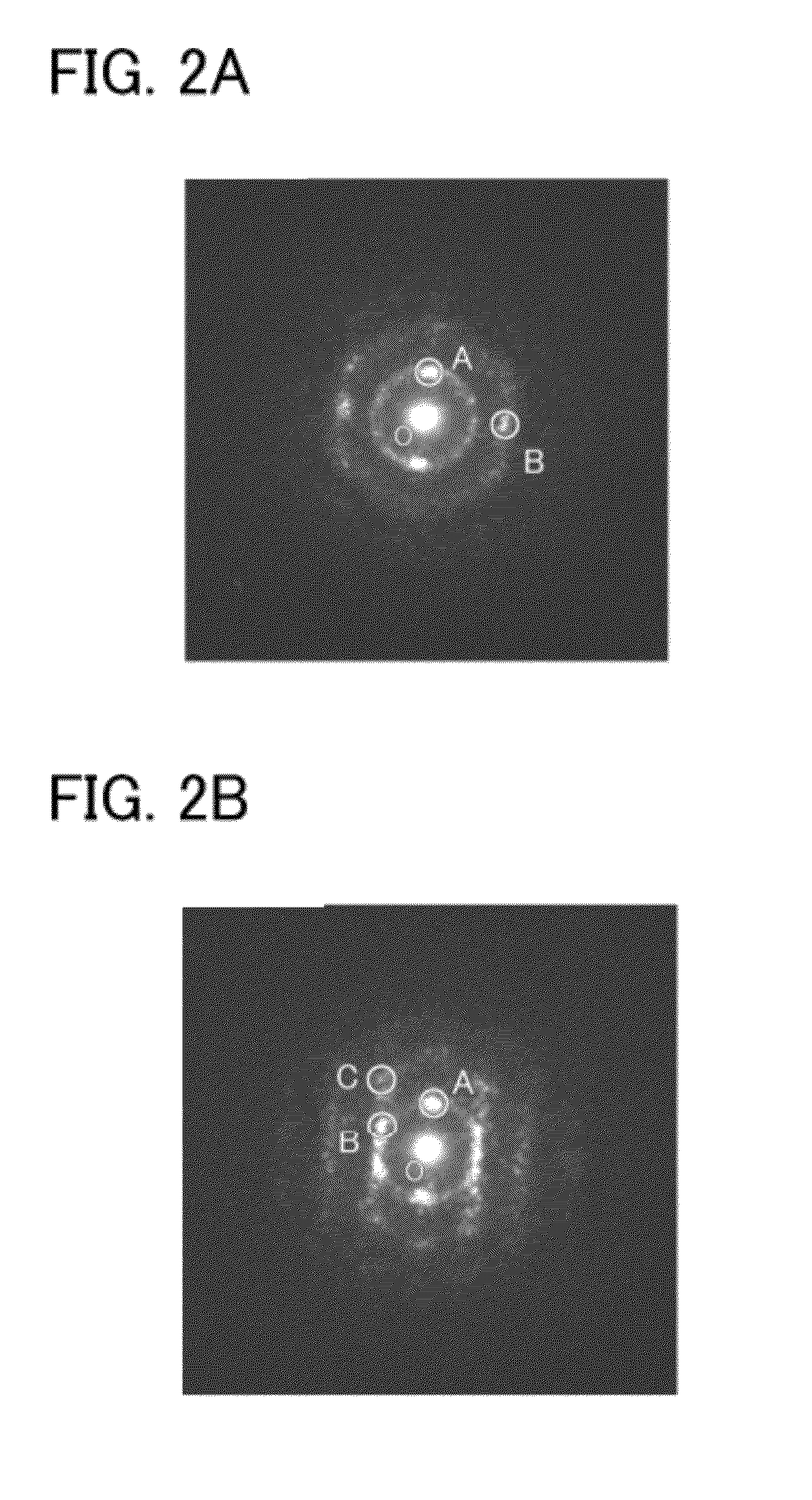
[0037]Here, an indium zinc oxide film having hexagonal and rhombohedral crystal structures was formed, and a cross section thereof was observed with a transmission electron microscope (TEM). FIG. 1 shows a result of the observation (cross-sectional TEM image). In the cross-sectional TEM image shown in FIG. 1, a plurality of regions can be seen in ...
embodiment 2
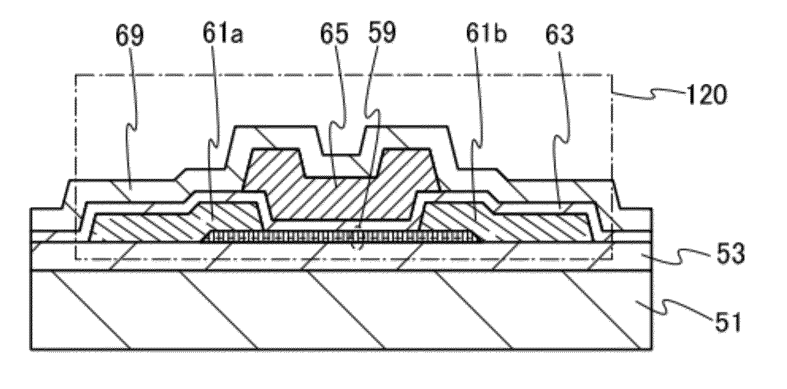
[0068]This embodiment shows a method of forming the indium zinc oxide film having hexagonal and rhombohedral crystal structures described in Embodiment 1 and a method of manufacturing a transistor including the indium zinc oxide film with reference to FIGS. 5A to 5E, FIGS. 6A and 6B, FIGS. 7A and 7B, FIGS. 8A and 8B, and FIGS. 9A to 9C. FIGS. 5A to 5E are cross-sectional views illustrating a process of manufacturing a top-gate transistor 120 which is an embodiment of the structure of a semiconductor device.
[0069]First, before the indium zinc oxide film having hexagonal and rhombohedral crystal structures is formed, a base insulating film 53 is preferably formed over a substrate 51 as illustrated in FIG. 5A.
[0070]The substrate 51 needs to have at least heat resistance high enough to withstand heat treatment performed later. When a glass substrate is used as the substrate 51, a glass substrate whose strain point is 730° C. or higher is preferably used. For a glass substrate, a glass m...
embodiment 3
[0149]In this embodiment, an example in which at least part of a driver circuit and a transistor to be disposed in a pixel portion are formed over one substrate is described below.
[0150]The transistor to be disposed in the pixel portion is formed in accordance with Embodiment 2. Further, the transistor can easily be an n-channel transistor; thus, part of a driver circuit that can be formed using an n-channel transistor in the driver circuit is formed over the same substrate as the transistor of the pixel portion. By using the transistor described in the above embodiment for the pixel portion or the driver circuit as described above, a highly reliable display device can be provided.
[0151]FIG. 10A is an example of a block diagram of an active matrix display device. A pixel portion 501, a first scan line driver circuit 502, a second scan line driver circuit 503, and a signal line driver circuit 504 are provided over a substrate 500 in the display device. In the pixel portion 501, a plu...
PUM
 Abstract
Description
Claims
Application Information