

Semiconductor device and manufacturing method thereof
a technology of semiconductor devices and dielectric layers, which is applied in the direction of semiconductor devices, basic electric elements, electrical appliances, etc., can solve the problems of reducing increasing the electric field strength inside the practical mos device, and affecting the performance of the device, so as to reduce parasitic resistance and capacitance, eliminate parasitic capacitance, and reduce parasitic resistance.
- Summary
- Abstract
- Description
- Claims
- Application Information
AI Technical Summary
Benefits of technology
Problems solved by technology
Method used
Image

Examples
Embodiment Construction
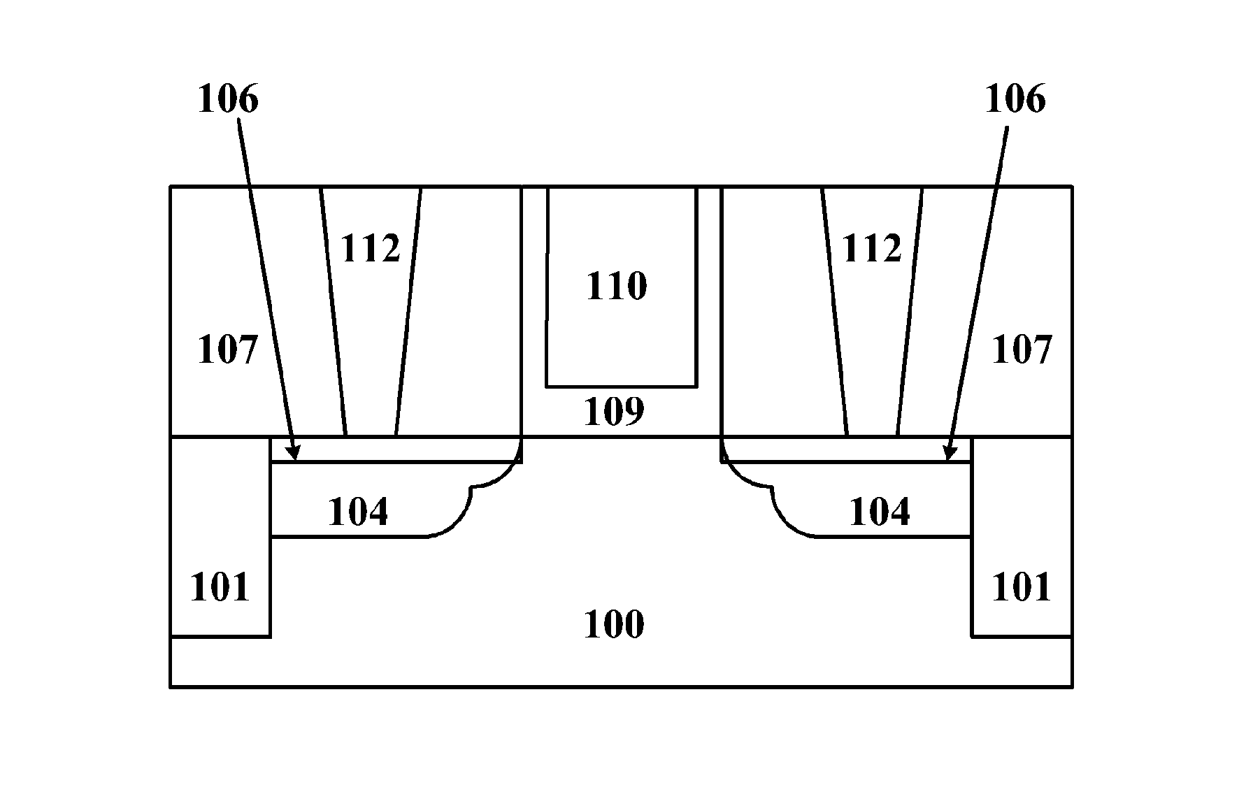
[0035]In the following the features and technical effects thereof of the technical solutions of the invention will be described in detail with reference to the accompanying drawings and in connection with exemplary embodiments of the invention. A novel semiconductor device structure and its manufacturing method is disclosed which can effectively reduce the RC delay. It needs to be noted that like reference numerals denote like structures, and the terms “first”, “second”, “above”, “below” and so on as used in this application can be used for describing various device structures. Such description does not suggest spatial, sequential or hierarchical relationship of the described device structures, unless specifically stated.
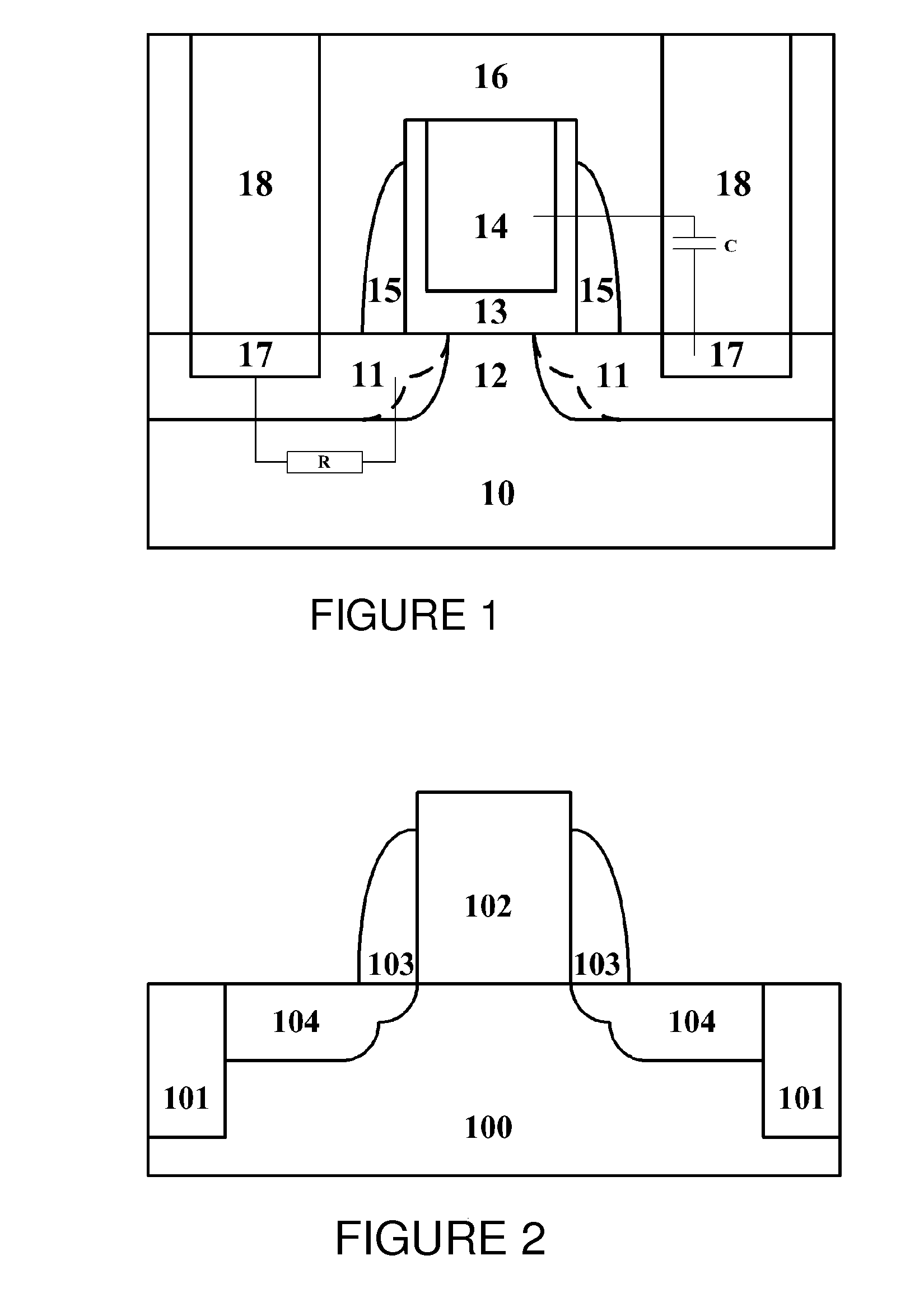
[0036]Firstly, heavily doped source / drain regions with an LDD structure are formed employing a conventional process. As shown in FIG. 2, a schematic cross section view of the LDD structure is shown. A thick oxide, e.g., silicon oxide, especially a silicon dioxide (S...
PUM
 Abstract
Description
Claims
Application Information