Methods for precleaning a substrate prior to metal silicide fabrication process

a technology of metal silicide and substrate, which is applied in the direction of semiconductor/solid-state device manufacturing, basic electric elements, electric apparatus, etc., can solve the problems of poor adhesion, adversely affecting the nucleation ability of metal elements, and substrate subject to oxidative conditions

Inactive Publication Date: 2012-11-01
APPLIED MATERIALS INC
View PDF18 Cites 11 Cited by
  • Summary
  • Abstract
  • Description
  • Claims
  • Application Information

AI Technical Summary

Problems solved by technology

As a result, the substrate can be subjected to oxidative conditions during the transfer, accumulating native oxides or contaminants on the substrate surface prior to the metal silicide fabrication process.
Excess native oxide accumulation or contaminants may adversely affect the nucleation capability of the metal elements to adhere on the substrate surface to form the metal silicide layer.
Poor nucleation of the metal elements on the interface may result in poor adhesion of the metal silicide layer to the silicon substrate surface, thereby resulting in peeling and particle flakes.
Furthermore, poor adhesion at the interface may also result in undesired high contact resistance, thereby resulting in poor electrical properties of the device characteristics.
In addition, poor nucleation of the metal elements adhered on the silicon substrate surface may further result in different stoichiometric ratios of metal elements to silicon elements formed in the resultant metal silicide layer, which may impact not only on the electrical performance of the devices, but also on the integration of the deposition of the conductive contact material subsequently formed thereon.

Method used


Image

  • Methods for precleaning a substrate prior to metal silicide fabrication process
  • Methods for precleaning a substrate prior to metal silicide fabrication process
  • Methods for precleaning a substrate prior to metal silicide fabrication process

Examples


Embodiment Construction

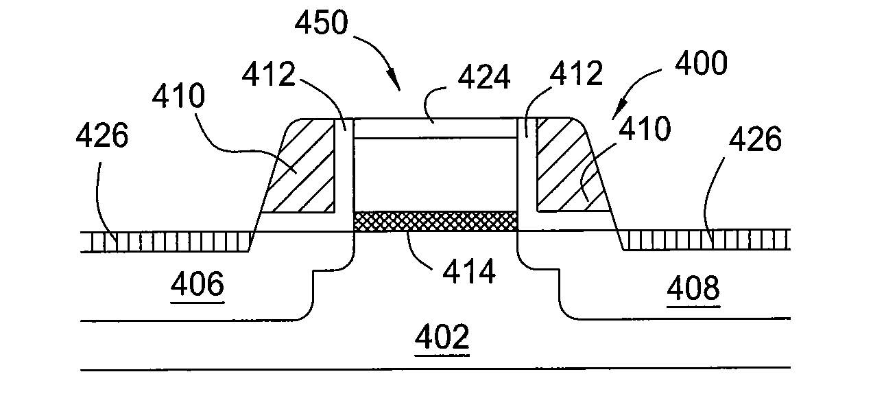
[0017]As will be explained in greater detail below, a substrate having a surface disposed thereon is treated to remove native oxides or other contaminants prior to forming a metal silicide layer thereon. The term “substrate” as used herein refers to a layer of material that serves as a basis for subsequent processing operations and includes a surface to be cleaned for forming a metal silicide layer thereon. For example, the substrate can include one or more conductive metals, such as aluminum, copper, tungsten, or combinations thereof. The substrate can also include one or more nonconductive materials, such as silicon, silicon oxide, doped silicon, germanium, gallium arsenide, glass, and sapphire. The substrate can also include dielectric materials such as silicon dioxide, organosilicates, and carbon doped silicon oxides. Further, the substrate can include any other materials such as metal nitrides and metal alloys, depending on the application. In one or more embodiments, the subst...


PUM

PropertyMeasurementUnit
diameteraaaaaaaaaa
diameteraaaaaaaaaa
pressureaaaaaaaaaa

Abstract

Methods for precleaning native oxides or other contaminants from a surface of a substrate prior to forming a metal silicide layer on the substrate. In one embodiment, a method for removing native oxides from a substrate includes transferring a substrate having an oxide layer disposed thereon into a processing chamber, performing a pretreatment process on the substrate by supplying a pretreatment gas mixture into the processing chamber, performing an oxide removal process on the substrate by supplying a cleaning gas mixture into the processing chamber, wherein the cleaning gas mixture includes at least an ammonium gas and a nitrogen trifluoride, and performing a post treatment process on the cleaned substrate by supplying a post treatment gas mixture into the processing chamber

Description

BACKGROUND OF THE INVENTION[0001]1. Field of the Invention[0002]Embodiments of the present invention generally relate to methods for forming semiconductor devices. More particularly, embodiments of the present invention generally relate to methods for pre-cleaning a substrate surface prior to forming a metal silicide on a semiconductor substrate.[0003]2. Description of the Related Art[0004]Metal gates or contacts typically include a doped silicon surface, one or more barrier layers, one or more liner layers and bulk metal to complete the gate structure. The cleanliness of the substrate surface between layers is critical for reducing contact resistance and hence, optimal device performance. For logic devices, the contact is usually a silicide, such as nickel silicide (NiSi), cobalt silicide (CoSi2), or titanium silicide (TiSi2). Nickel silicide is becoming more popular for smaller geometries, e.g., geometries having aspect ratios of about 10:1 or smaller, because NiSi is widely avail...

Claims


Application Information

Patent Timeline
Patent Type & Authority Applications(United States)
IPC IPC(8): H01L21/3205
CPCH01L21/0206H01L21/02068H01L21/67207H01L21/28518H01L21/28506
Inventor ZHENG, BOSUNDARRAJAN, ARVINDHAMKAR, MANISH
Owner APPLIED MATERIALS INC
Why Eureka
Try Eureka