Sic epitaxial wafer and method for manufacturing same

a technology of epitaxial wafers and manufacturing methods, applied in the direction of crystal growth process, polycrystalline material growth, chemically reactive gases, etc., can solve the problems of stacking faults, step bunching, performance enhancement approaching its limits, etc., to improve the uniformity of carrier concentration and film thickness, and the effect of satisfactory in-plane uniformity

Inactive Publication Date: 2012-11-08
SHOWA DENKO KK
View PDF6 Cites 76 Cited by
  • Summary
  • Abstract
  • Description
  • Claims
  • Application Information

AI Technical Summary

Benefits of technology

[0093]According to the foregoing configuration, it is possible to offer a step-bunching-free SiC epitaxial wafer of particularly high quality compared to conventional wafers, which reduces triangular defects and stacking faults, which improves uniformity of carrier concentration and film thickness, and which has no step bunching over the entire surface of the wafer, and a method of manufacture thereof.
[0094]By fabricating an electronic device using a high-quality SiC epitaxial wafer of the foregoing configuration which has few triangular defects and stacking faults, which has satisfactory in-plane uniformity, and which is free of step bunching, the effects of property stability and property enhancement of the electronic device, as well as yield improvement are obtained.
[0095]By conducting epitaxial growth of silicon carbide film (1) in the case of use of a 4H—SiC single crystal substrate with an off angle of 0.4°

Problems solved by technology

Power electronics has undergone technological improvement and performance enhancement using conventional silicon (Si) semiconductors, but it is said that performance enhancement is approaching its limits due to limits on the material and physical properties of silicon.
Incorporation of different polytypes disturbs the laminar structure of the crystal lattice, causing stacking faults.
In order to inhibit such incorporation, epitaxial growth is ordinarily conducted by slightly tilting the SiC single crystal substrate, and conducting step-flow growth (lateral growth from an atomic step), but steps of high growth rate overtake and combine with steps of slow growth rate, causing step bunching.
However, because the terrace width of the surface of the SiC single crystal substrate (wafer) increases as the off-angle decreases, irregularities tend to occur in the rate of introduction of the migrating atoms that are introduced at the step edges, i.e., the growth rate of the step edges.
As a result, there is the problem that steps of high growth r

Method used


Image

  • Sic epitaxial wafer and method for manufacturing same
  • Sic epitaxial wafer and method for manufacturing same
  • Sic epitaxial wafer and method for manufacturing same

Examples


working examples

[0187]The present invention is described in further detail below by means of working examples, but the present invention is not limited by these working examples.

[0188]The present working examples use SiH4 gas as the silicon-containing gas, C3H8 gas as the carbon-containing gas, N2 gas as the doping gas, and H2 gas as the carrier gas and the etching gas, and SiC epitaxial film is grown on an Si surface and a C surface which are slightly tilted in the axis direction relative to the (0001) surface of the 4H—SiC single crystal by a Hot Wall SiC CVD (VP2400HW) manufactured by Aixtron Corporation which is a multiple-sheet planetary (autorotation) CVD apparatus of the mass production type.

[0189]Si Surface of 4H—SiC Single Crystal Substrate with Off Angle of 4°

working example 1

[0190]An SiC epitaxial layer was grown on the Si surface of a 4H—SiC single crystal substrate tilted at an off angle of 4°.

[0191]In the present working example, convexity machining is not conducted on the 4H—SiC single crystal substrate.

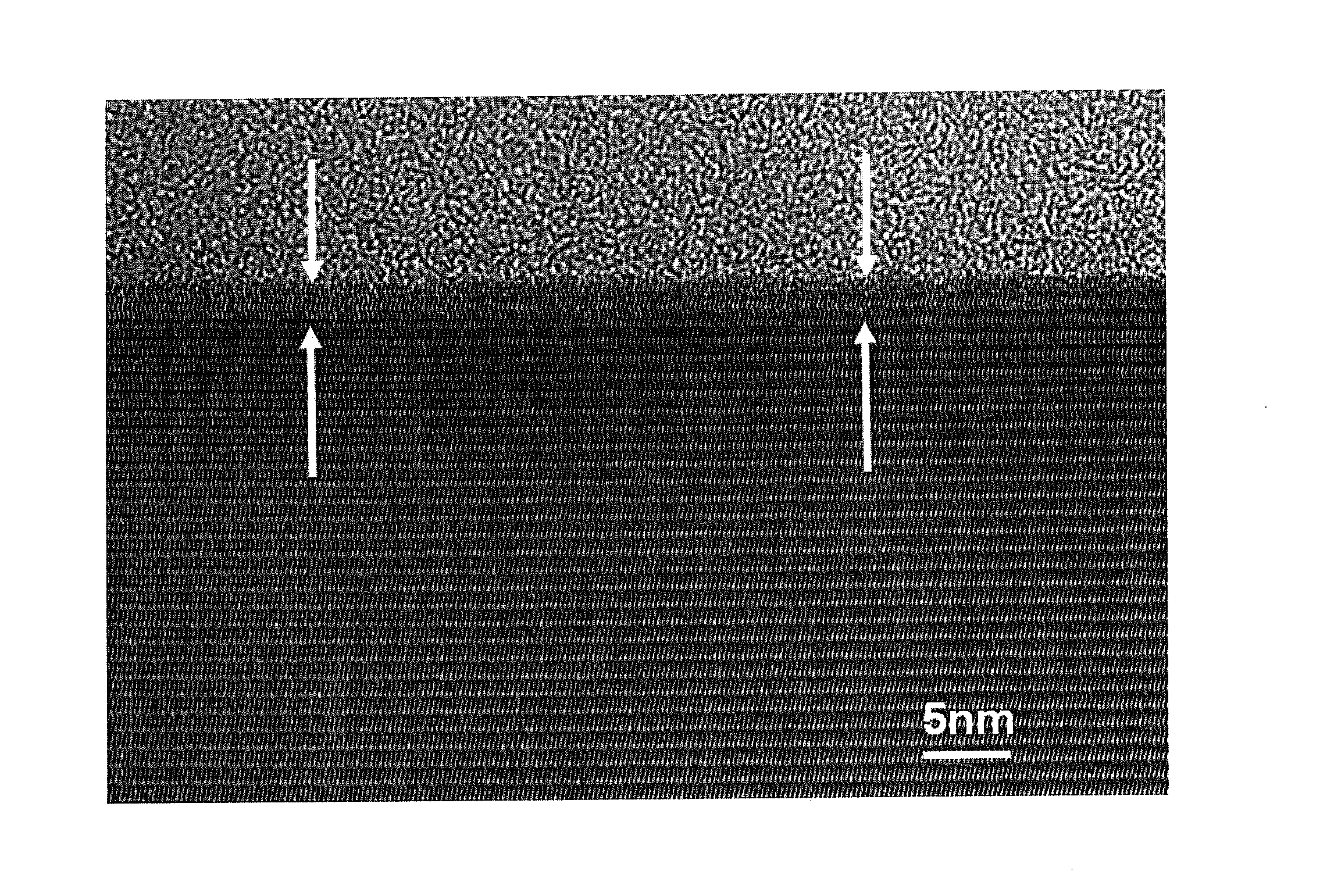
[0192]With respect to the polishing process, the mechanical polishing prior to CMP was conducted at a working pressure of 350 g / cm2, using abrasive grain with a diameter of 5 μm or less. CMP was conducted for 30 minutes under conditions where silica particles with an average particle size of 10-150 nm were used as the polishing particles, sulfuric acid was included as the inorganic acid, and a polishing slurry with a pH of 1.9 at 20° C. was used. By this means, the lattice disorder layer of the surface was 3 nm or less.

[0193]After polishing, the substrate was subjected to RCA cleaning, and subsequently introduced into the growth apparatus. RCA cleaning is a wet cleaning method which is commonly used on Si wafers, and is able to remove organic matter ...

working example 2

[0203]An SiC epitaxial wafer was manufactured under the same manufacturing conditions as Working Example 1, except that the growth process was conducted for 2.5 hours at a growth rate of 4 μm / h.

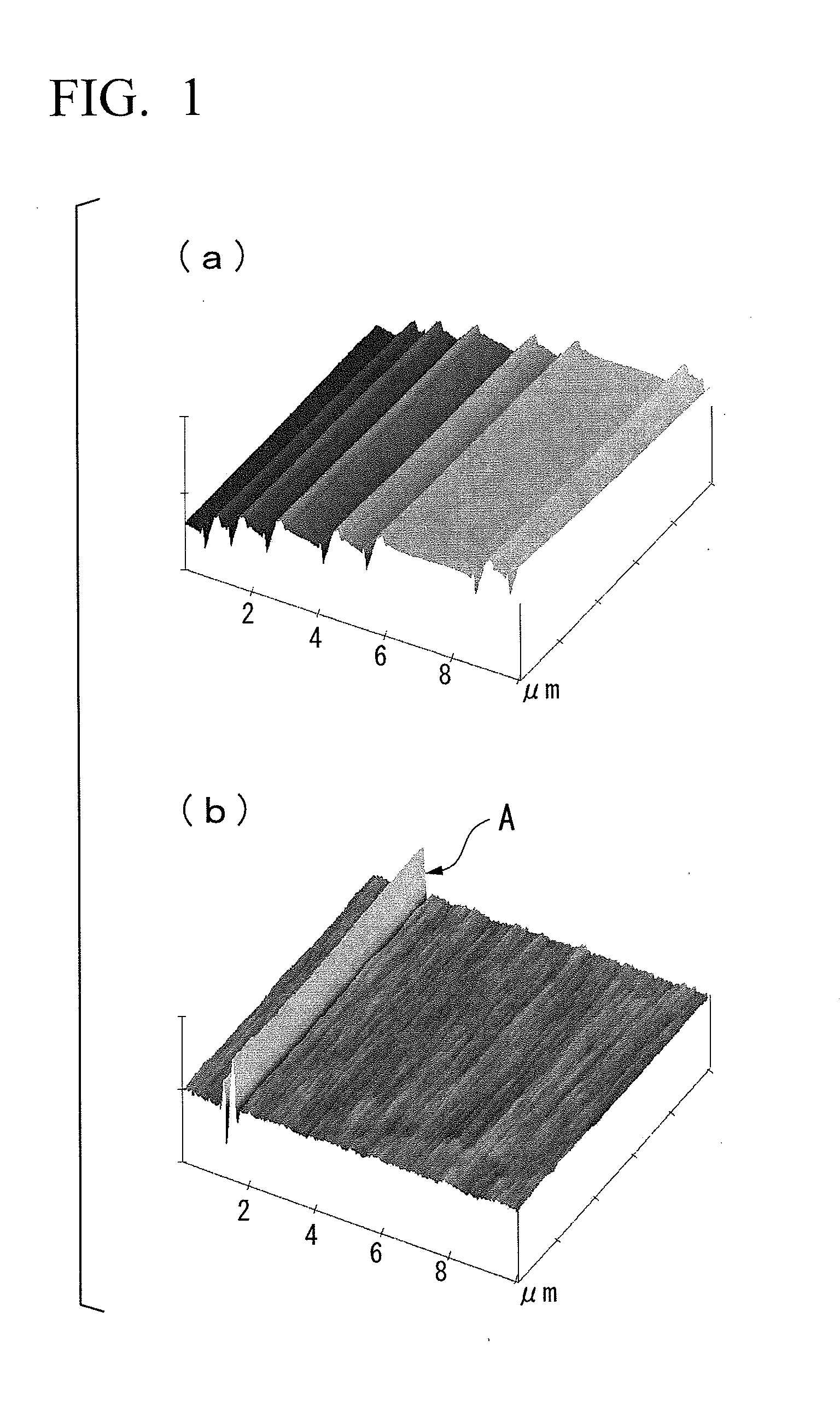
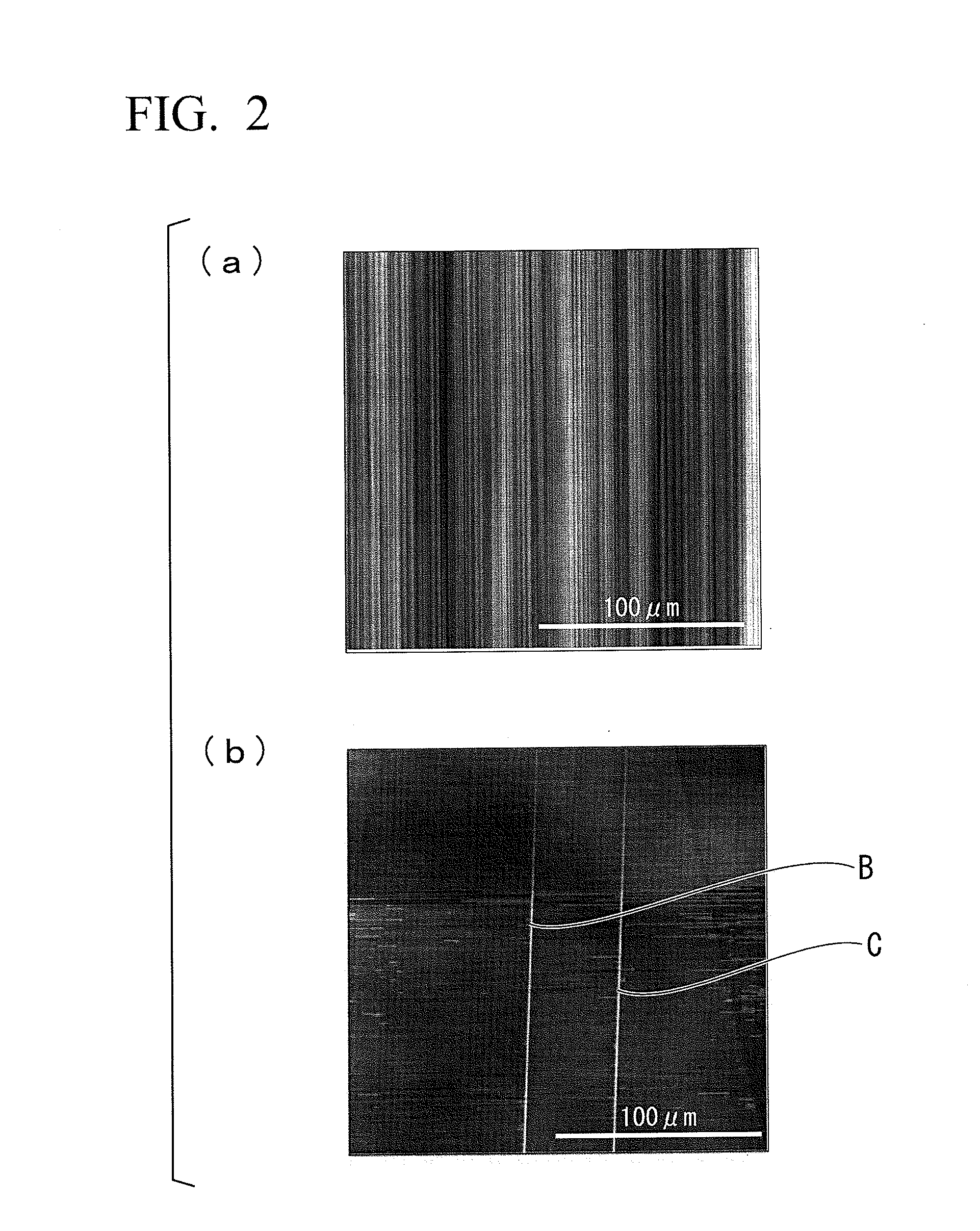
[0204]The manufactured SiC epitaxial wafer was measured and evaluated by an optical surface inspection device (Candela CS20 manufactured by KLA-Tencor Corporation) and a photoluminescence imaging device (PLI-100 manufactured by Photon Design Corporation), and a wide-range observation type AFM (Nanoscale Hybrid Microscope VN-8000 manufactured by Keyence Corporation).

[0205]Triangular defect density was 0.4 defects / cm2, and stacking fault density was 0.1 faults / cm2. No step bunching was observed.

[0206]Both cases were under 1 defect or fault / cm2, and even with respect to a 4H—SiC single crystal substrate with a 1.2° off angle lower than that of Working Example 1, extremely high quality epitaxial film of low defect density was formed.

[0207]C Surface of 4H—SiC Single Crystal Substrate with Off Angl...


PUM

PropertyMeasurementUnit
Temperatureaaaaaaaaaa

Abstract

According to the present invention, there is provided an SiC epitaxial wafer which reduces triangular defects and stacking faults, which is highly uniform in carrier concentration and film thickness, and which is free of step bunching, and its method of manufacture. The SiC epitaxial wafer of the present invention is an SiC epitaxial wafer in which an SiC epitaxial layer is formed on a 4H—SiC single crystal substrate that is tilted at an off angle of 0.4°-5°, wherein the density of triangular-shaped defects of said SiC epitaxial layer is 1 defect/cm2 or less.

Description

TECHNICAL FIELD[0001]The present invention relates to an SiC epitaxial wafer and its method of manufacture. Specifically, it relates to a high-quality SiC epitaxial wafer which has low defect density, which is highly uniform in film thickness and carrier concentration, and which is free of step bunching, and to its method of manufacture.[0002]Priority is claimed on Japanese Patent Application No. 2009-283113, filed Dec. 14, 2009, the content of which is incorporated herein by reference.BACKGROUND ART[0003]In response to the problem of global warming, there is demand for enhancement of energy conservation technology. Among the many technological matters being treated, power electronics technology which reduces energy loss during power conversion is situated as a core technology. Power electronics has undergone technological improvement and performance enhancement using conventional silicon (Si) semiconductors, but it is said that performance enhancement is approaching its limits due ...

Claims


Application Information

Patent Timeline
IPC IPC(8): H01L29/161H01L21/20
CPCC30B25/186C30B29/36H01L21/02378H01L21/02433H01L21/02529H01L29/1608H01L21/02661C30B25/02C30B25/16C30B25/165H01L29/045H01L21/0262C23C16/42C30B25/20H01L21/205
Inventor MUTO, DAISUKEMOMOSE, KENJIODAWARA, MICHIYA
Owner SHOWA DENKO KK
Why Eureka
Try Eureka