Material for a molded resin for use in a semiconductor light-emitting device

a technology of light-emitting devices and molded resins, which is applied in the direction of lighting and heating apparatus, camera filters, instruments, etc., can solve the problems of reduced light-emitting efficiency of semiconductor light-emitting devices, inability to meet the requirements of lighting, so as to achieve strong light resistance, improve led output, and high durability

Inactive Publication Date: 2012-11-15
MITSUBISHI CHEM CORP
View PDF9 Cites 20 Cited by
  • Summary
  • Abstract
  • Description
  • Claims
  • Application Information

AI Technical Summary

Benefits of technology

[0039]A highly durable (strongly light resistant and heat resistant) molded resin for a semiconductor light-emitting device, that also brings about an improved LED output through its excellent reflectivity, can be obtained using the material of the present invention for a molded resin. Moreover, the present invention provides an easy-to-mold material for a molded resin for a semiconductor light-emitting device.

Problems solved by technology

Even when a white pigment is used in Patent Document 1, its reflection efficiency may not be satisfactory depending on the particular type of white pigment, and light absorbed in the molded resin and light penetrating through the molded resin also ultimately escape.
Due to this, it has not been possible in some cases to concentrate the light from the semiconductor light-emitting element in the desired direction and the light-emitting efficiency of the semiconductor light-emitting device has been reduced as a result.
Polyamides are thermoplastic resins, and polyamides are thus softened by this heat and the heat resistance of the package then becomes a problem in the case of packages that use polyamide.
Furthermore, polyamides are subject to photodegradation and thermal degradation by ultraviolet radiation and heat, and degradation by light has become a problem in particular when light-emitting elements are used that have a light-emission range that extends into high-energy wavelength regions, such as the blue to near-ultraviolet semiconductor light-emitting elements whose commercialization has been ongoing in the recent years.
Moreover, thermal degradation and photodegradation have become even more significant problems due to the heat and high luminous flux light generated by the semiconductor light-emitting element as a result of contemporary demands for brighter light-emitting elements.
This sintering step has posed the following problems: cost problems due, for example, to electricity costs; the ease of appearance of defective products due to changes in the size and shape of the molding caused by sintering; and an impaired productivity.

Method used


Image

  • Material for a molded resin for use in a semiconductor light-emitting device
  • Material for a molded resin for use in a semiconductor light-emitting device
  • Material for a molded resin for use in a semiconductor light-emitting device

Examples


example 1

Synthesis of Polyorganosiloxane (1)

[0232]A vinyl group-containing polydimethylsiloxane (vinyl group content: 1.2 mmol / g, viscosity adjusted to 1000 mPa·s by the addition of finely divided silica particles, contained 6.8 ppm of a platinum complex catalyst) and a hydrosilyl group-containing polydimethylsiloxane (vinyl group content: 0.3 mmol / g, hydrosilyl group content: 1.8 mmol / g, viscosity adjusted to 2100 mPa·s by the addition of finely divided silica particles) were mixed at 1:1 to obtain a liquid heat-curable polyorganosiloxane (1) having a viscosity of 1500 mPa·s and a platinum concentration of 3.4 ppm.

[0233]The finely divided silica particles corresponded to the fluidity controlling agent (E) and were added at a polyorganosiloxane: finely divided silica particle (weight ratio) of from 80:20 to 89.5:10.5 to provide the viscosities indicated above.

Synthesis of Polyorganosiloxane (2)

[0234]A vinyl group-containing polydimethylsiloxane (vinyl group content: 0.3 mmol / g, viscosity: 35...

example 10

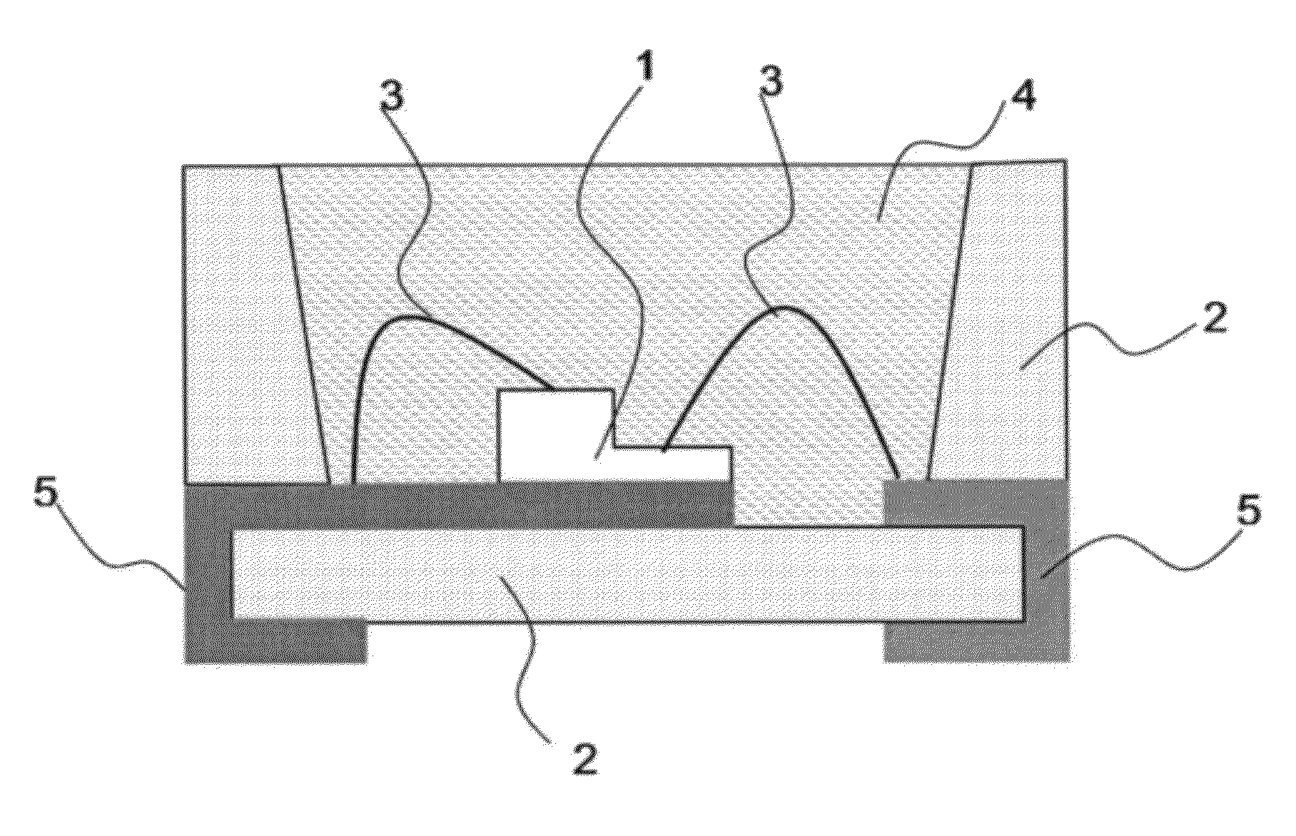
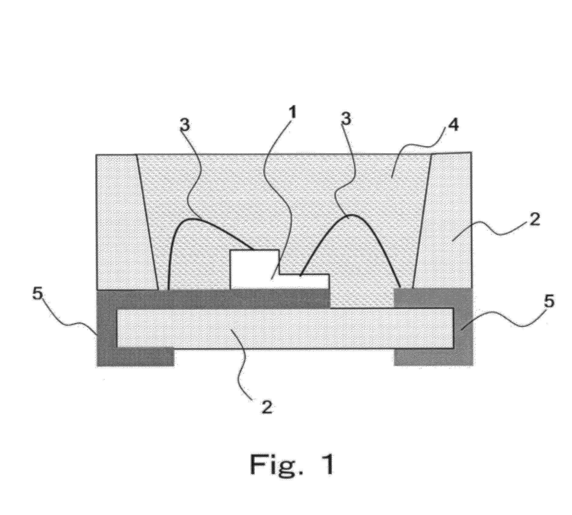
[0254]A package for a semiconductor light-emitting device was molded by liquid injection molding using the material of Example 3 in combination with a copper lead frame that had been silver plated over its entire surface. This package was a cup-shaped surface-mount package with the resin portion having length 3.2 mm×width 2.7 mm×height 1.4 mm and a concave portion with a diameter of 2.4 mm for the opening. Molding was performed for a curing time of 20 seconds at a mold temperature of 170° C. Observation of the molded package showed the package to be free of flash and free of short molding.

example 11

[0255]A package for a semiconductor light-emitting device was molded by liquid injection molding using the material of Example 3 in combination with a copper lead frame that had been silver plated over its entire surface. This package was a cup-shaped surface-mount package having length 5 mm×width 5 mm×height 1.5 mm and a concave portion with a diameter of 3.6 mm for the opening. Molding was performed for a curing time of 180 seconds with a 150° C. mold. The molded package was sectioned with a microtome while frozen with liquid nitrogen and the package cross section was observed by SEM. The primary particle diameter of the alumina exposed in the cross section was 0.3 μm and the primary particle aspect ratio was 1.42.


PUM

PropertyMeasurementUnit
median diameteraaaaaaaaaa
viscosityaaaaaaaaaa

Abstract

The present invention provides a material for a molded resin as a material for a semiconductor light-emitting device that can yield a highly durable (light resistance and heat resistance) molded resin and can also improve the LED output through an excellent reflectivity. The present invention also provides an easily moldable material for a molded resin for a semiconductor light-emitting device. The material for a molded resin for a semiconductor light-emitting device is a resin composition comprising (A) a polyorganosiloxane, (B) a white pigment, and (C) a curing catalyst, wherein the white pigment (B) has the following characteristics (a) and (b); (a) an aspect ratio 1.2 or more and 4.0 or less, and (b) a primary particle diameter 0.1 μm or more and 2.0 μm or less.

Description

TECHNICAL FIELD[0001]The present invention relates to a material for a molded resin that is used in a semiconductor light-emitting device that has a light-emitting element, for example, a light-emitting diode, and to a molding made of the material.BACKGROUND ART[0002]As shown in FIG. 1, a semiconductor light-emitting device made, by mounting a semiconductor light-emitting element is composed of, for example, a semiconductor light-emitting element 1, a molded resin 2, a bonding wire 3, an encapsulant 4, and a lead frame 5. The structure comprising the electroconductive metal interconnects, e.g., the lead frame, and the insulating molded resin is referred to as the package.[0003]Insulating materials provided by incorporating a white pigment in a thermoplastic resin, e.g., a polyamide, have already entered into general use as insulating materials used for molded resins (refer, for example, to Patent Document 1). In the case of semiconductor light-emitting devices where directionality i...

Claims


Application Information

Patent Timeline
Patent Type & Authority Applications(United States)
IPC IPC(8): G02B5/26
CPCC08L83/04H01L33/56H01L2224/49107H01L2224/48247H01L2224/48091H01L2933/0091C08K3/36C08G77/12C08G77/20C08K5/56C08K2003/2227C08L83/00H01L2924/00014C08K2201/016
Inventor TAKASU, MAYUKOOTSU, TAKESHITAKIZAWA, KENICHIMORI, YUTAKA
Owner MITSUBISHI CHEM CORP
Why Eureka
Try Eureka