
Sers substrates

a substrate and raman spectroscopy technology, applied in the field of materials science, surface engineering, spectroscopy, can solve the problems of ser commercial application, impede the use of sers, and produce significant changes in the raman signal, and difficult quantitative or even semi-quantitative analysis

Inactive Publication Date: 2012-11-15
LI HAO +2
View PDF4 Cites 33 Cited by
  • Summary
  • Abstract
  • Description
  • Claims
  • Application Information

AI Technical Summary

Problems solved by technology

However, there are technical and non-technical challenges in fabrication of SERS substrates that significantly impede the commercial applications of SERS.
For example, most existing SERS substrates exhibit inconsistent activities and it is a common problem that a subtle change in the substrate manufacturing process can produce significant changes of the Raman signal.
Such inconsistencies make quantitative or even semi-quantitative analysis difficult.

Method used


Image

  • Sers substrates
  • Sers substrates
  • Sers substrates

Examples


example 1

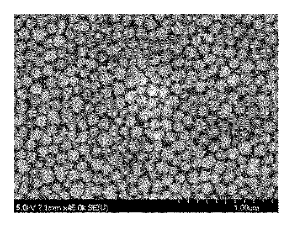
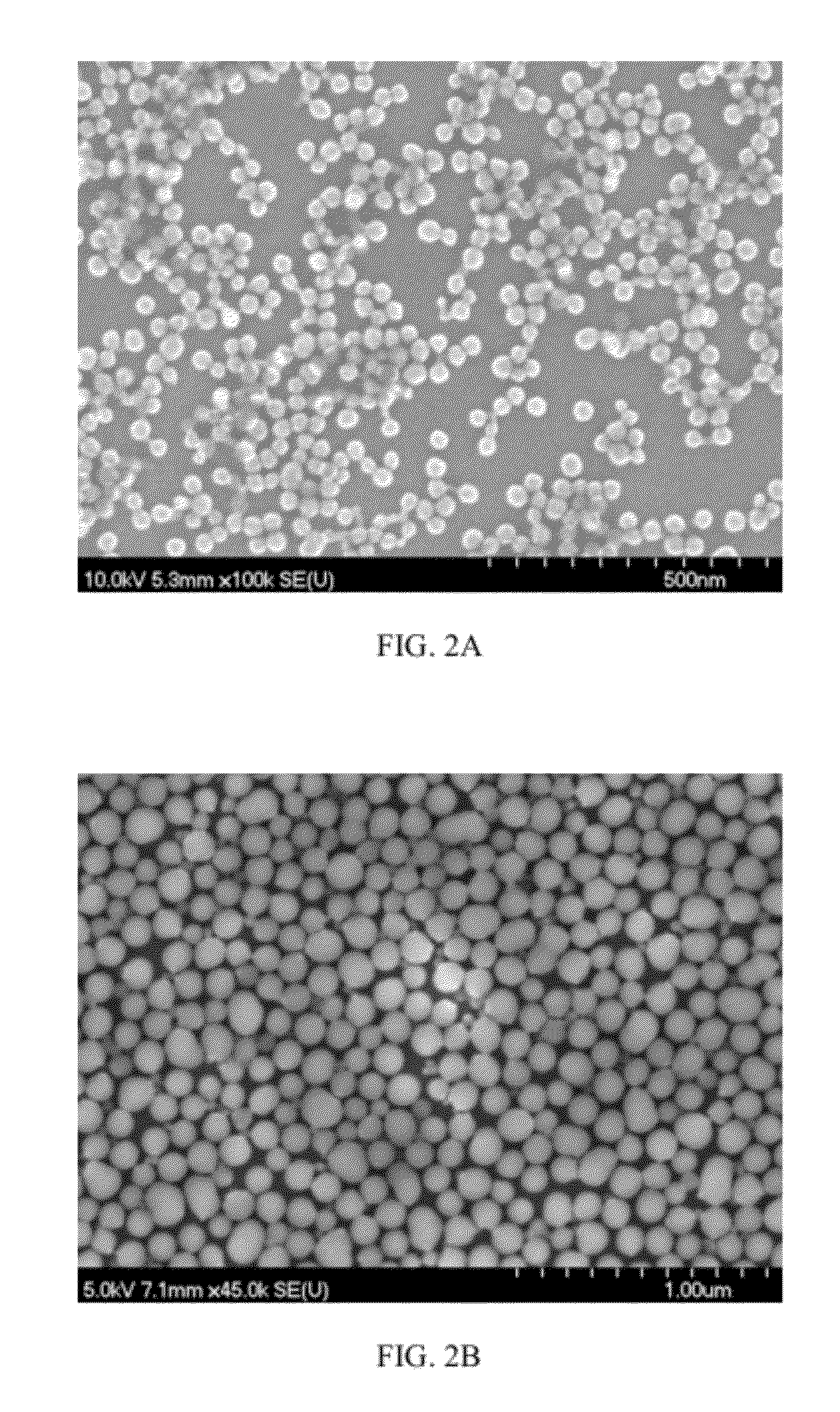
[0032]An aqueous colloidal suspension of SiO2 nanoparticles (20-100 nm) of concentration between about 0.5%-5% may be prepared by adding a predetermined quantity of SiO2 to water or by diluting high a highly concentrated colloidal suspension of SiO2 with water. Magnetic stirring can be used to achieve better dispersion of the silica nanoparticles. Droplets of SiO2 nanoparticle colloidal suspension may be used to coat a Si wafer, such as by using a spin coater. FIGS. 2A-2C show formation of an incomplete silica nanoparticle monolayer, a complete SiO2 nanoparticle monolayer, and a double-layer SiO2 nanoparticle coating, respectively, on Si wafers. After the coating process, a gold coating containing gold nanoparticles (10-20 nm) may be applied on the SiO2 nanoparticle coatings. FIG. 3 shows a typical SEM image of an Au nanoparticle-coated SiO2 nanoparticle coating. The Au coating thickness typically may range from 10 nm to 50 nm. After the deposition of Au coating, the substrate becom...

example 2

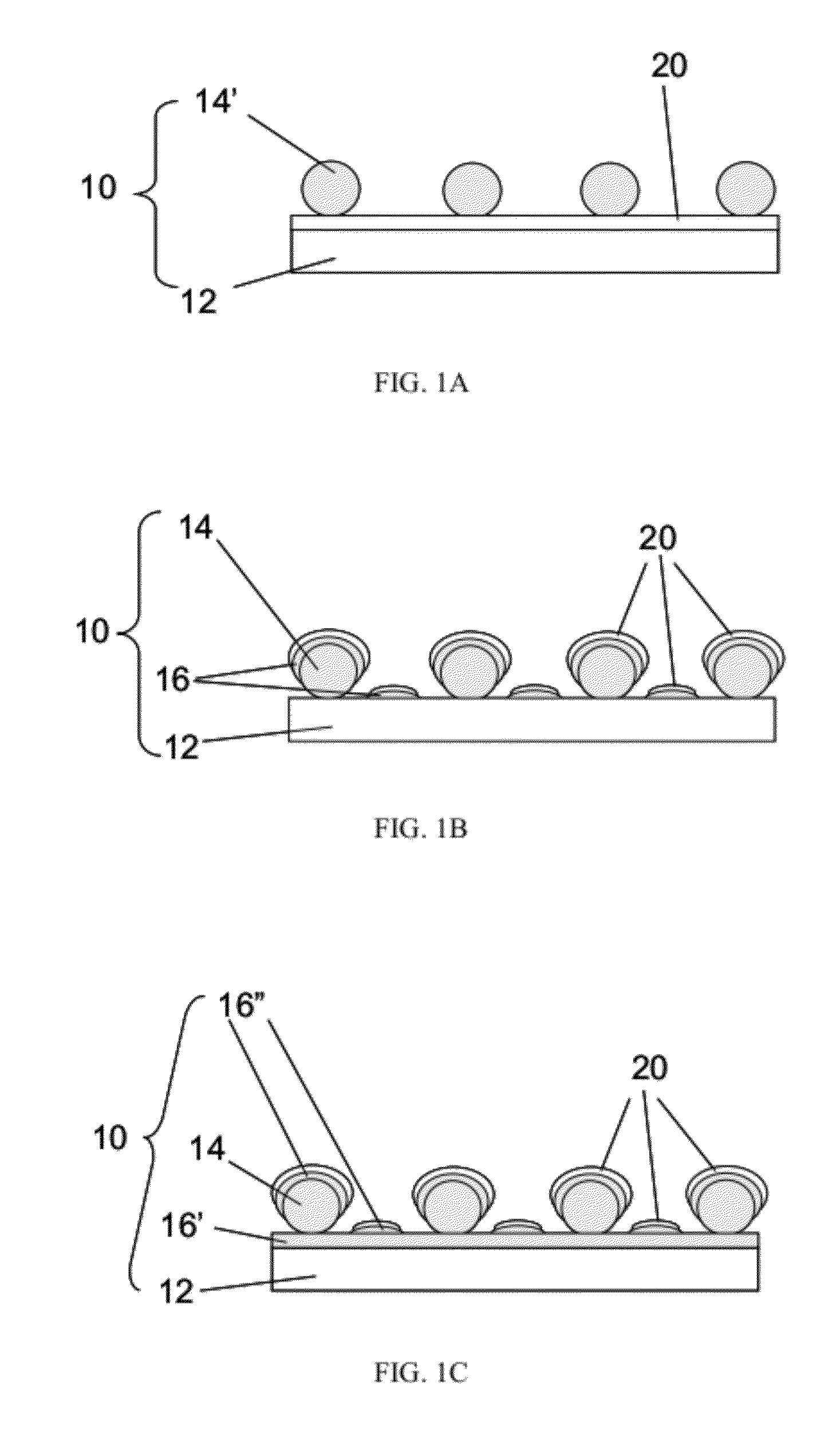
[0034]FIG. 7 shows one example of multiple layered SERS active nanostructures 14. The first layer Au coating 16′ was sputtered onto a glass substrate and a second layer Ag nanocubes 14′ was dip-coated onto the Au coated glass substrate 12. Coverage of the second Ag nanocube coating 14′ is controllable by concentration and / or other techniques, and the Ag nanocubes 14′ may also be applied via a spin coating technique. It is expected that the Au nanoparticles 16′ and Ag nanocubes 14′ may work best with different laser wave lengths and may be sensitive to different chemicals. Such a combination coating may allow for the fabrication of SERS substrates 10 tailored for unique and enhanced performance and sensitivity as compared to traditional SERS substrates or even substrates 10 having uniform nanostructure layers of the same metal or metal alloy. In addition, the different nanostructures 16′, 14′ may interact with each other to improve the enhancement factors, such as by creating hot-spo...


PUM


Abstract

A surface-enhanced Raman spectroscopy substrate device, including a base substrate, a single or multiple layered nanostructure that contains metals, and a plasma coating. The nanostructure metal is selected from the group including silver, gold, platinum, copper, titanium, chromium, and combinations thereof. The plasma coating has a thickness of 1-200 nm and may locate on the nanostructure layer or on the base substrate. The plasma coating can precisely control the surface characteristics, including surface energy, hydrophilicity, and contact angle, of the SERS device and may then help to regulate the SERS substrate with well defined and uniform water / oil contact angle with small standard deviation. The water contact angle of the SERS substrate may range from 20 to 140 degrees.

Description

TECHNICAL FIELD[0001]The present invention relates generally to materials science, surface engineering, spectroscopy, and, more particularly, surface enhanced Raman spectroscopy (SERS).BACKGROUND[0002]Optical-based sensing has several major advantages over electronic sensing because optical sensing reveals spectral fingerprints of chemical compounds rapidly and accurately, thus significantly simplifying the detection process and reducing false alarms. One of the most promising optical sensing techniques is surface enhanced Raman spectroscopy (SERS), which employs noble metal nanostructures to dramatically enhance Raman signals. With the aid of metallic nanostructures, such as gold- or silver-based nanosubstrates, a Raman signal can be enhanced by 104 to 108 times or even higher. This enhancement is due to the generation of spatially localized surface Plasmon resonance (SPR) “hot spots” where huge local enhancements of electromagnetic field are obtained. The location of “hot spots” o...

Claims


Application Information

Patent Timeline
IPC IPC(8): G01J3/44B82Y15/00B82Y20/00
CPCB82Y15/00G01N21/658Y10S977/811G01N2201/06113Y10S977/773B82Y20/00
Inventor LI, HAOLIN, MENGSHIYU, QINGSONG
Owner LI HAO
Learn More