Method and process for metallic stamp replication for large area nanopatterns
- Summary
- Abstract
- Description
- Claims
- Application Information
AI Technical Summary
Benefits of technology
Problems solved by technology
Method used
Image

Examples
experimental examples
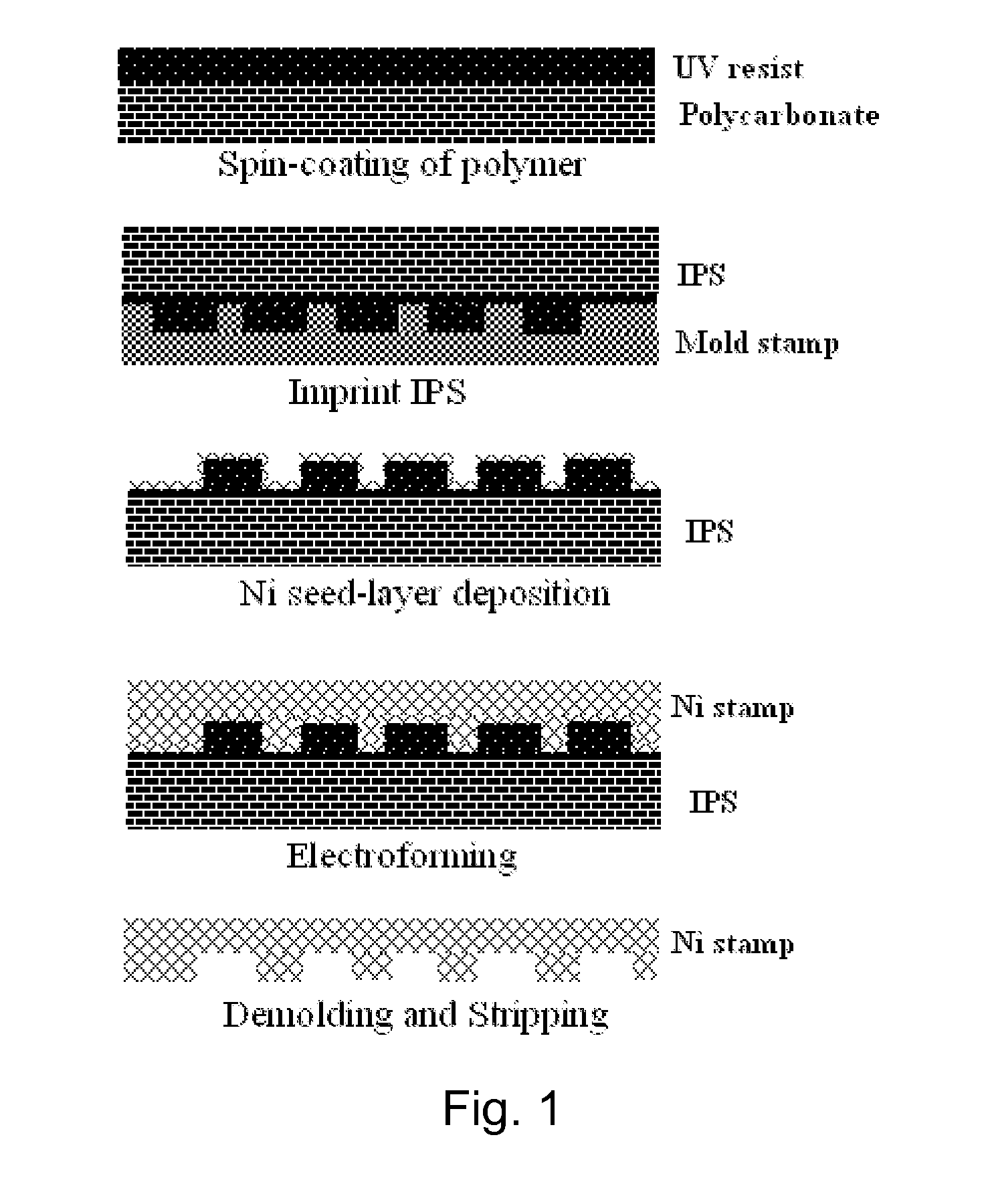
Fabrication Process for Ni-Stamp Replication from the IPS
example 1
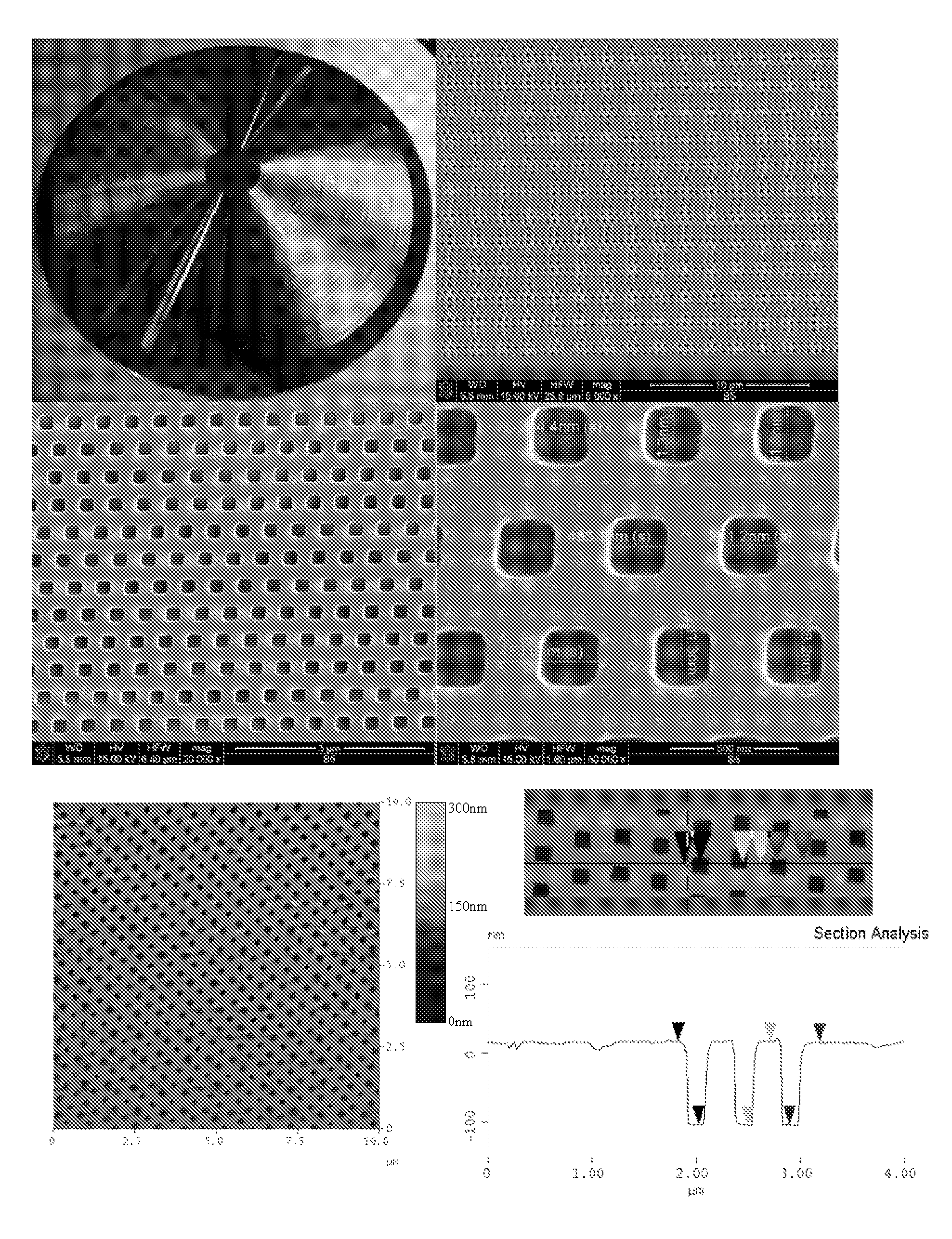
Nickel Stamp with Photonic Crystal Structures (PCS)
[0032]The original master stamp was obtained, for instance, by a combined e-beam recording (EBR) and electroforming process. A nickel stamp obtained in this fashion consists of an array of width 230 nm PCS with a pitch of 450 nm and a depth of 130 nm across 4-inch patterned area. An acrylate imprint resist was coated onto a polycarbonate polymer sheet and then used as the substrate for nanoimprinting. After demoulding the IPS, it was inspected by AFM, SEM and an optical microscope. The surface of the IPS was further modified by depositing a thin (˜6 nm) fluorocarbon film via plasma enhanced chemical vapor deposition. Then, a nickel seed layer was sputtered onto the IPS prior to electroforming. The thickness of the sputtered Ni-seed layer was 10 nm. Since we adopted nickel as the seed layer, the definition of the nanostructures should be maintained well. It could be seen that the replicated nickel-stamp has identical structures to th...
example 2
Nickel Stamp with Magnetic Storage Media Nanostructures
[0033]An original nickel imprint was produced by a combined e-beam recording technique and an electroforming process. In a data track area the patterns have dimensions of 40 nm in width and 120 nm in pitch. The imprinted IPS was inspected with SEM, using an acrylate imprint resist on a polycarbonate polymer sheet. The inverse nanofeatures were transferred with good fidelity. After sputtering of a thin film (˜10 nm) of nickel, the electroforming was performed. The big advantage of sputtering a thin metal layer instead of thick layer is to avoid hole-inclusion due to narrow nanochannels with high aspect ratio and with high pattern density. The electroformed nickel stamp with nanostructures identical to those of the original master stamp was obtained (FIG. 4).
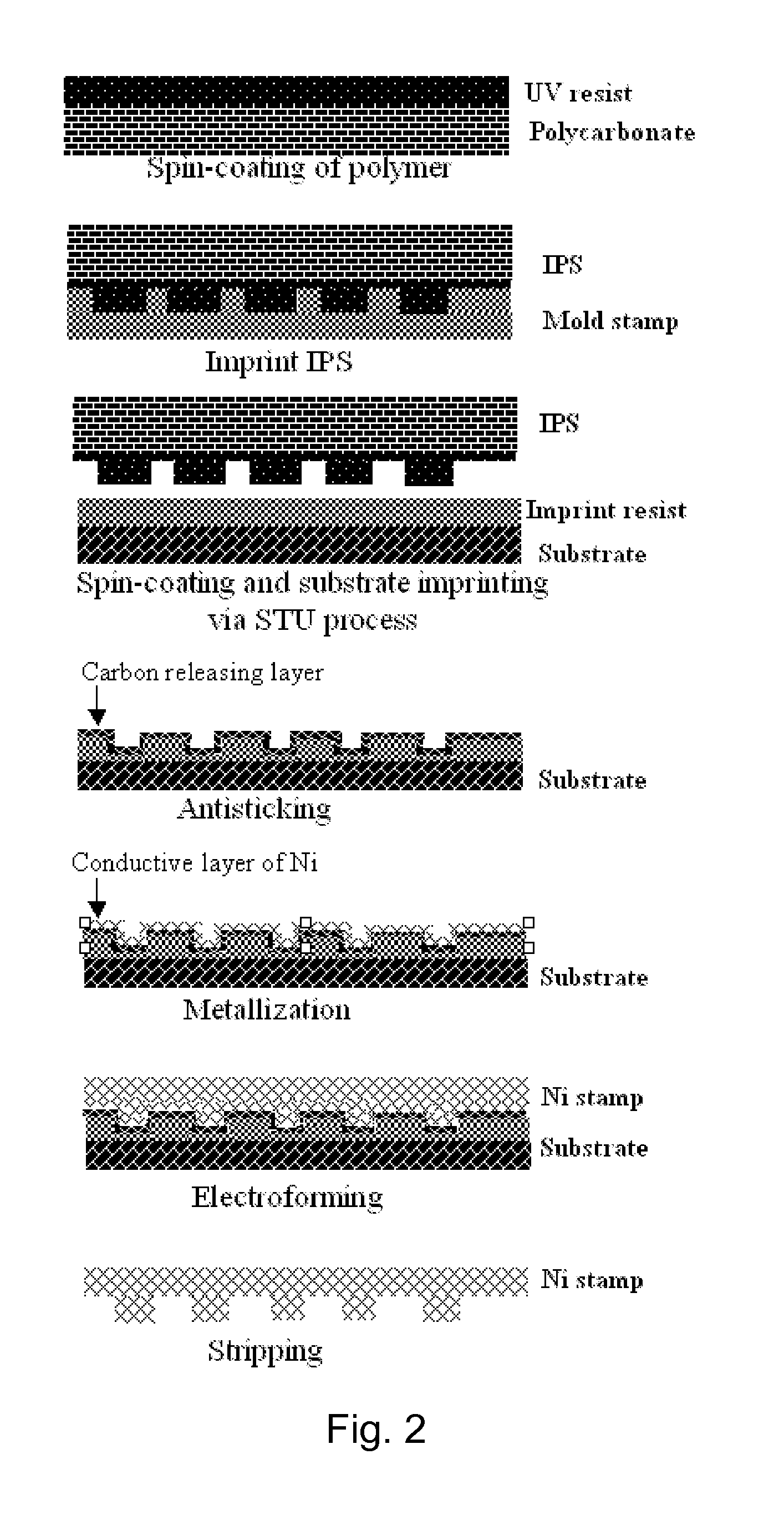
Fabrication Process for Ni-Stamp Replication from the Two-Step Imprint
PUM
| Property | Measurement | Unit |
|---|---|---|
| Temperature | aaaaa | aaaaa |
| Size | aaaaa | aaaaa |
| Thickness | aaaaa | aaaaa |
Abstract
Description
Claims
Application Information
 - R&D Engineer
- R&D Manager
- IP Professional
- Industry Leading Data Capabilities
- Powerful AI technology
- Patent DNA Extraction
Browse by: Latest US Patents, China's latest patents, Technical Efficacy Thesaurus, Application Domain, Technology Topic.
© 2024 PatSnap. All rights reserved.Legal|Privacy policy|Modern Slavery Act Transparency Statement|Sitemap