Interleaved Bit Line Architecture for 2T2C Ferroelectric Memories

a ferroelectric memory and interleaved bit line technology, applied in the field of solid-state memories, can solve the problems of essentially volatile devices, conventional mos capacitors losing their stored charge, and the realization of a full memory array of 2t2c memory cells, in combination with corresponding sense amplifiers, becomes difficult as device feature sizes continue to shrink

Inactive Publication Date: 2012-12-06
TEXAS INSTR INC
View PDF2 Cites 91 Cited by
  • Summary
  • Abstract
  • Description
  • Claims
  • Application Information

AI Technical Summary

Benefits of technology

[0018]Embodiments of this invention provide a non-volatile solid-state memory of the two-transistor, two-capacitor ferroelectric type in which coupling among bit lines of adjacent columns is reduced.

Problems solved by technology

As is fundamental in the art, however, those devices are essentially volatile, in that logic and memory circuits constructed according to these technologies do not retain their data states upon removal of bias power.
In contrast, conventional MOS capacitors lose their stored charge on power-down of the device.
However, it has been observed, in connection with this invention, that the realization of a full memory array of 2T2C memory cells, in combination with corresponding sense amplifiers, is becoming difficult as device feature sizes continue to shrink.
As known in the art, a signal transition of one polarity occurring at one bit line in a closely-packed memory array can couple to an adjacent bit line for a neighboring column; if that adjacent bit line is making a transition of the opposite polarity, the induced noise from its neighbor can cause a data error.
This noise-coupling problem is exacerbated with shrinking memory cell sizes, because of the corresponding reduction in signal strength from the smaller memory cells, and because of the close proximity of adjacent bit lines to one another.
This bit line twisting of course complicates the layout of the memory array, and consumes chip area.
Another limitation encountered in modern 2T2C ferroelectric memories involves the layout constraints on sense amplifier circuitry.
These defects are reflected in degraded data retention performance (i.e., degraded non-volatility) for these edge cells.
It is believed that these increased edge cell defects are caused by hydrogen from the ambient atmosphere during fabrication being absorbed by the ferroelectric material, such as PZT, in capacitors at the array edge to a greater extent than by capacitors in the array interior.

Method used


Image

  • Interleaved Bit Line Architecture for 2T2C Ferroelectric Memories
  • Interleaved Bit Line Architecture for 2T2C Ferroelectric Memories
  • Interleaved Bit Line Architecture for 2T2C Ferroelectric Memories

Examples


Embodiment Construction

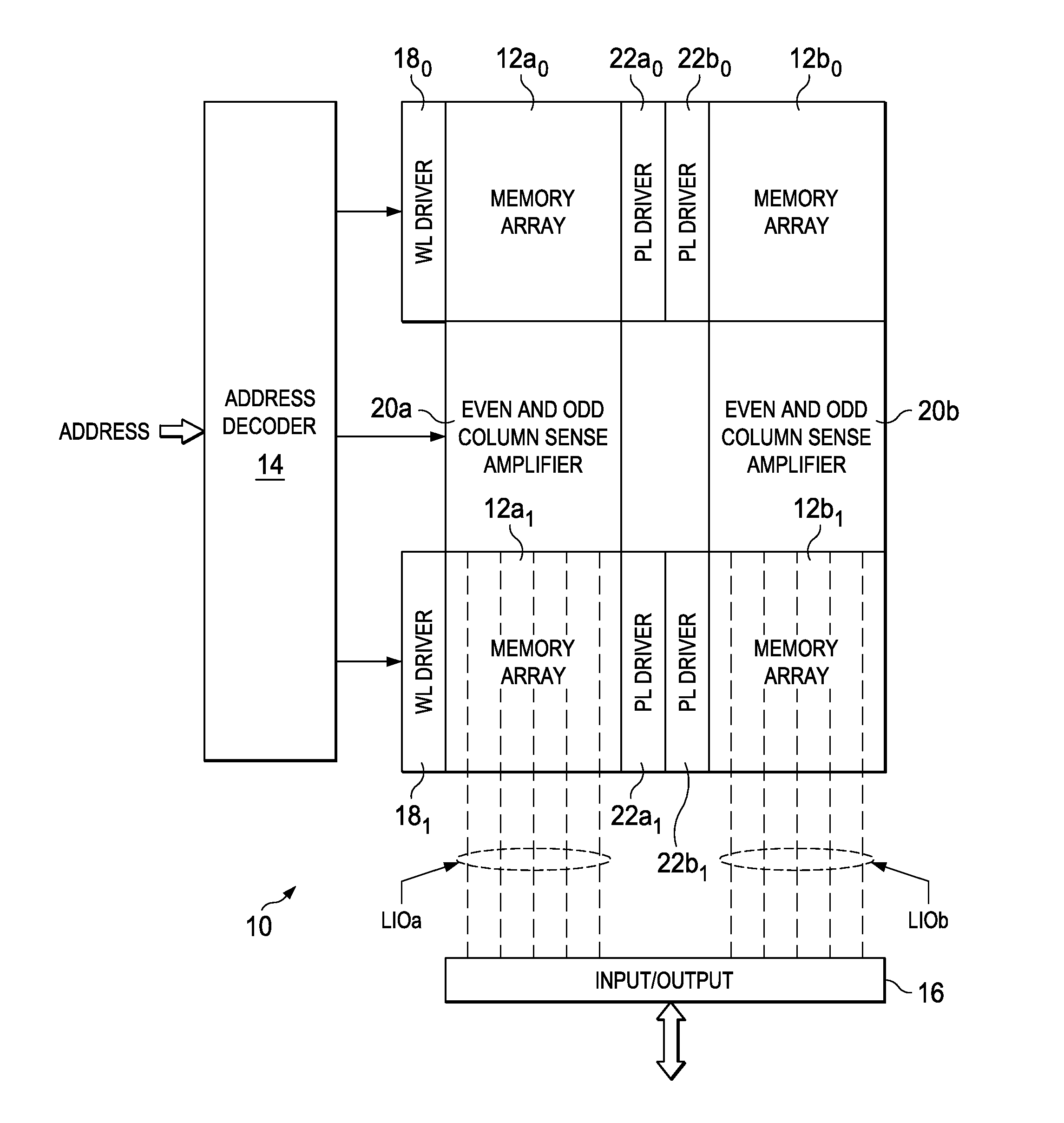
[0031]This invention will be described in connection with its embodiments, namely as implemented into an integrated circuit incorporating one or more arrays of ferroelectric random access memory (RAM) cells, as it is contemplated that this invention is especially beneficial in such an application. It is also contemplated that this invention may provide important benefits in other types of integrated circuits. Accordingly, it is to be understood that the following description is provided by way of example only, and is not intended to limit the true scope of this invention as claimed.

[0032]FIG. 4 illustrates the architecture of memory 10 constructed according to embodiments of this invention. In this example, memory 10 is shown as a stand-alone ferroelectric memory device (i.e., constructed as an FRAM). It is also contemplated that memory 10 may alternatively be integrated into a large-scale logic device such as a microprocessor, single-chip microcomputer, or a so-called “system-on-a-...


PUM


Abstract

A ferroelectric memory with interleaved pairs of ferroelectric memory cells of the two-transistor, two-capacitor (2T2C) type. Each memory cell in a given pair is constructed as first and second portions, each portion including a transistor and a ferroelectric capacitor. Within each pair, a first portion of a second memory cell is physically located between the first and second portions of the first memory cell. As a result, complementary bit lines for adjacent columns are interleaved with one another. Each sense amplifier is associated with a multiplexer, so that the adjacent columns of the interleaved memory cells are supported by a single sense amplifier. Noise coupling among the bit lines is reduced, and the sense amplifiers can be placed along one side of the array, reducing the number of dummy cells required to eliminate edge cell effects.

Description

CROSS-REFERENCE TO RELATED APPLICATIONS[0001]Not applicable.STATEMENT REGARDING FEDERALLY SPONSORED RESEARCH OR DEVELOPMENT[0002]Not applicable.BACKGROUND OF THE INVENTION[0003]This invention is in the field of solid-state memories as realized in semiconductor integrated circuits. Embodiments of this invention are more specifically directed to the construction of arrays of ferroelectric memory cells in such memories.[0004]Conventional metal-oxide-semiconductor (MOS) and complementary MOS (CMOS) logic and memory devices are prevalent in modern electronic devices and systems, as they provide an excellent combination of fast switching times and low power dissipation, along with their high density and suitability for large-scale integration. As is fundamental in the art, however, those devices are essentially volatile, in that logic and memory circuits constructed according to these technologies do not retain their data states upon removal of bias power. Especially in mobile and miniatu...

Claims


Application Information

Patent Timeline
Patent Type & Authority Applications(United States)
IPC IPC(8): G11C11/22
CPCG11C11/221
Inventor MCADAMS, HUGH P.SUMMERFELT, SCOTT R.NDAI, PATRICK M.
Owner TEXAS INSTR INC
Why Eureka
Try Eureka