
Method for fabricating a dram capacitor

a dram capacitor and capacitor body technology, applied in the direction of capacitors, semiconductor devices, electrical equipment, etc., can solve the problems of high leakage current in the device, increase in the eot and/or device leakage, and undesirable high temperature processes in the manufacture of dram devices

Inactive Publication Date: 2012-12-06
INTERMOLECULAR +1
View PDF7 Cites 17 Cited by
  • Summary
  • Abstract
  • Description
  • Claims
  • Application Information

AI Technical Summary

Benefits of technology

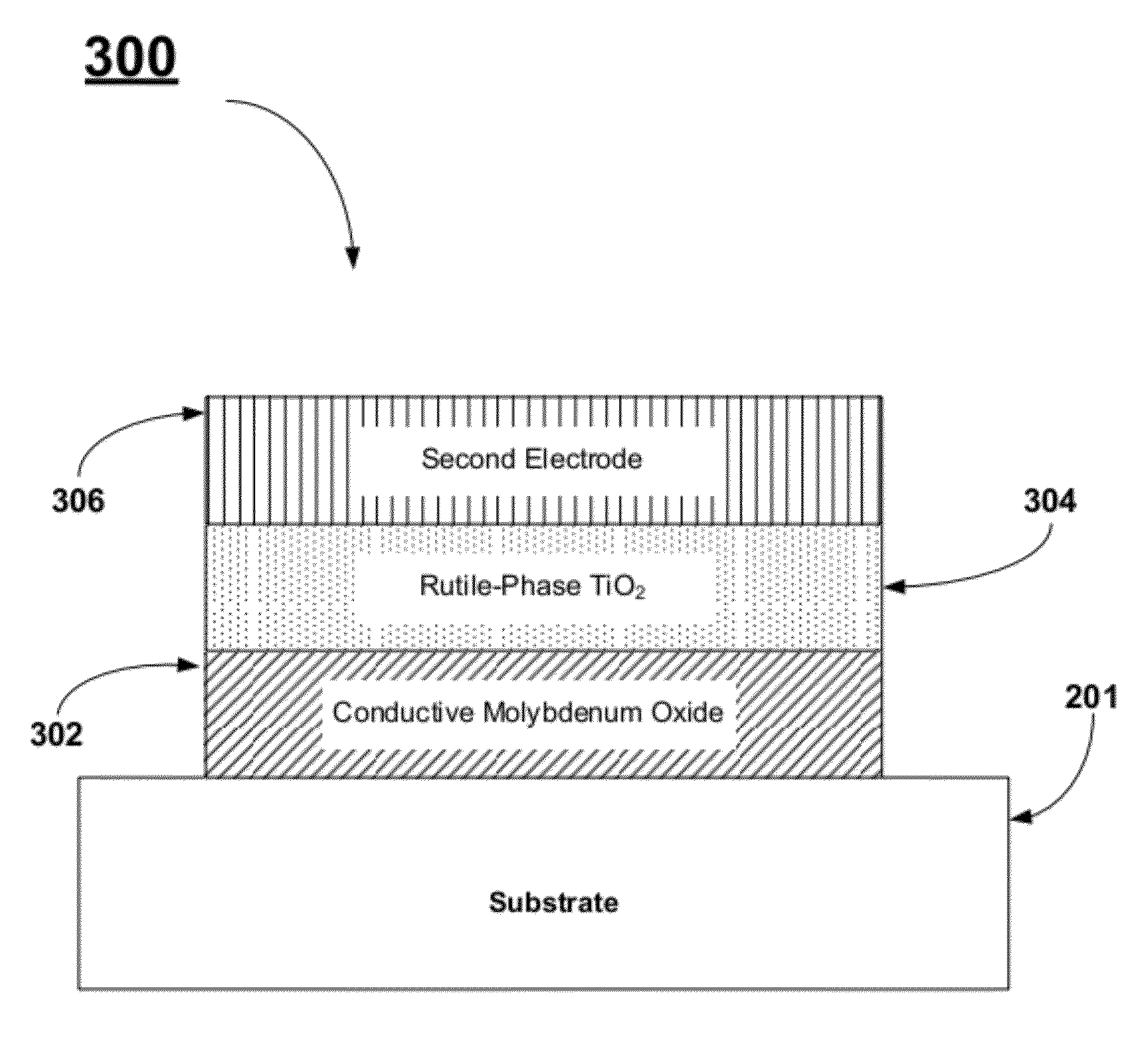
"The patent text discusses a joint research agreement between Intermolecular, Inc. and Elpida Memory, Inc. The technical effect of the patent is to improve the performance of dynamic random access memory (DRAM) by developing new electrode materials and dielectric materials for the DRAM capacitors. The goal is to maintain a large cell capacitance and low leakage current while reducing the size of the capacitors in the integrated circuit. The use of high-k materials with higher conductivity and stability over semiconductor materials is necessary for faster device speeds. The dielectric constant of a dielectric material is dependent upon its crystalline phase, so it is desirable to produce TiO2 based DRAM capacitors with the rutile-phase to increase the physical thickness of the layer while maintaining the same desired capacitance. The use of high-k materials in MIM capacitors is necessary to reduce the leakage current and improve the electrical performance of the dielectric material."

Problems solved by technology

However, high temperature processes are undesirable in the manufacture of DRAM devices.
The degradation may lead to an increase in the EOT and / or increased device leakage.
This leads to high leakage current in the device.
As a result, without the utilization of countervailing measures, capacitor stacks implementing high-k dielectric materials may experience large leakage currents.
The noble metal systems, however, are prohibitively expensive when employed in a mass production context.
Moreover, electrodes fabricated from noble metals often suffer from poor manufacturing qualities, such as surface roughness, poor adhesion, and form a contamination risk in the fab.
However, oxygen-rich phases (MoO2+x) of MoO2 degrade the performance of the MoO2 electrode because they act more like insulators and have crystal structures that do not promote the deposition of the rutile-phase of TiO2.

Method used


Image

  • Method for fabricating a dram capacitor
  • Method for fabricating a dram capacitor
  • Method for fabricating a dram capacitor

Examples


Embodiment Construction

[0031]It is to be understood that both the foregoing general description and the following detailed description are exemplary and explanatory only and are not restrictive of the invention as claimed. The accompanying drawings, which are incorporated in and constitute a part of the specification, illustrate embodiments of the invention and together with the general description, serve to illustrate the principles of the invention. Reference will now be made in detail to the subject matter disclosed, which is illustrated in the accompanying drawings.

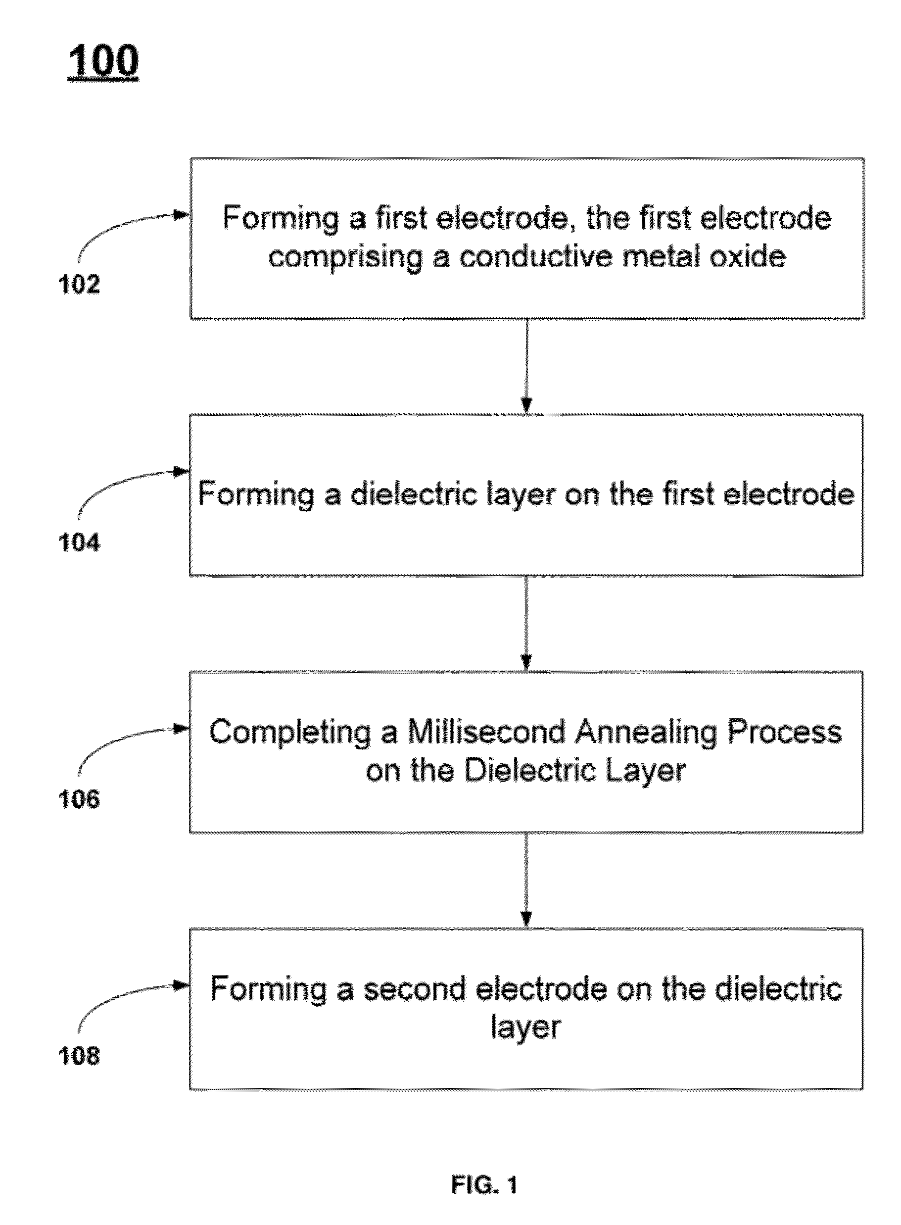
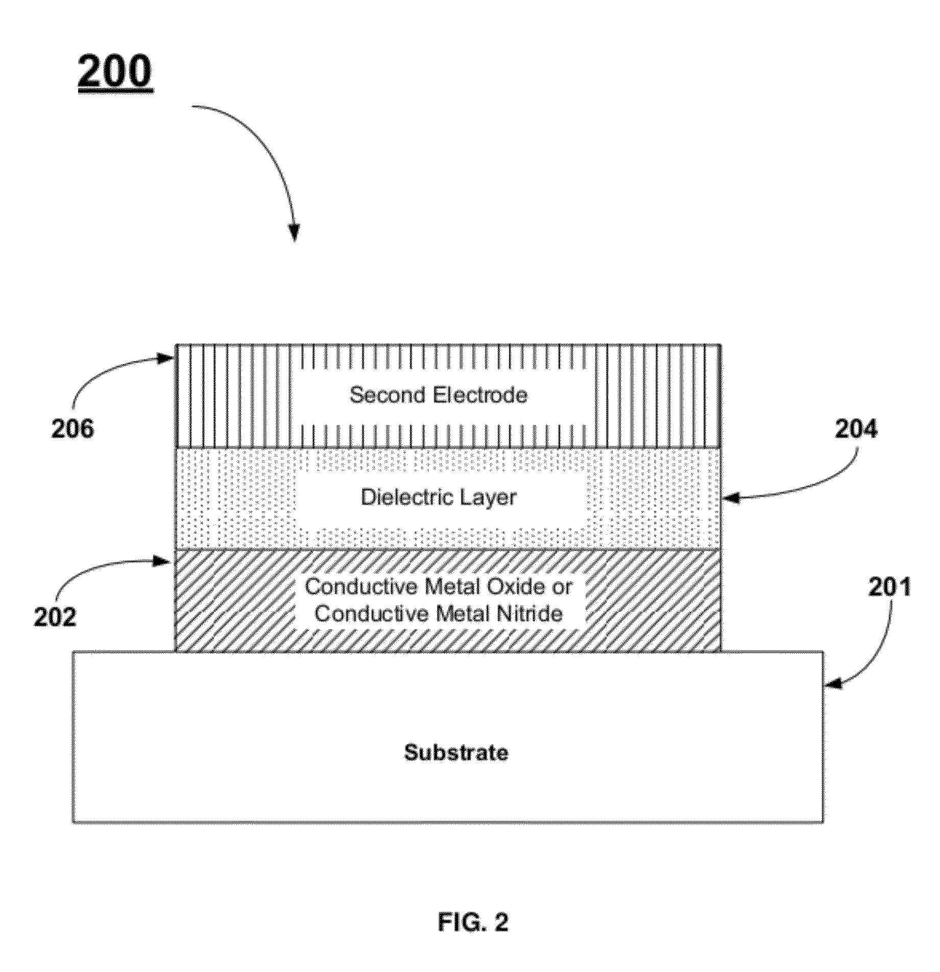
[0032]FIG. 1 describes a method, 100, for fabricating a DRAM capacitor stack. The initial step, 102, comprises forming a first electrode layer. Examples of suitable electrode materials comprise conductive metal oxides, conductive metal silicides, conductive metal nitrides, or combinations thereof. Two particularly interesting classes of materials are the conductive metal oxides and conductive metal nitrides. The next step, 104, comprises fo...


PUM

PropertyMeasurementUnit
temperatureaaaaaaaaaa
work functionaaaaaaaaaa
cell capacitanceaaaaaaaaaa

Abstract

A method for fabricating a dynamic random access memory (DRAM) capacitor stack is disclosed wherein the stack includes a first electrode, a dielectric layer, and a second electrode. The first electrode is formed from a conductive binary metal. A dielectric layer is formed over the first electrode. The dielectric layer is subjected to a milliseconds anneal process that serves to crystallize the dielectric material and decrease the concentration of oxygen vacancies.

Description

[0001]This document relates to the subject matter of a joint research agreement between Intermolecular, Inc. and Elpida Memory, Inc.FIELD OF THE INVENTION[0002]The present invention generally relates to the field of dynamic random access memory (DRAM), and more particularly to electrode processing for improved DRAM performance.BACKGROUND OF THE INVENTION[0003]Dynamic Random Access Memory utilizes capacitors to store bits of information within an integrated circuit. A capacitor is formed by placing a dielectric material between two electrodes formed from conductive materials. A capacitor's ability to hold electrical charge (i.e., capacitance) is a function of the surface area of the capacitor plates A, the distance between the capacitor plates d (i.e. the physical thickness of the dielectric layer), and the relative dielectric constant or k-value of the dielectric material. The capacitance is given by:C=κɛ0Ad(Eqn.1)where ∈o represents the vacuum permittivity.[0004]The dielectric cons...

Claims


Application Information

Patent Timeline
Patent Type & Authority Applications(United States)
IPC IPC(8): H01L21/02H10N97/00
CPCH01L28/40H01L29/92H01L28/65H01L28/60
Inventor RAMINI, KARTHIKODE, HIROYUKIMALHOTRA, SANDRA
Owner INTERMOLECULAR
Learn More