Scanning signal line drive circuit and display device having the same

a drive circuit and signal line technology, applied in the direction of digital storage, instruments, computing, etc., can solve the problem that the source bus line cannot transmit video signals indicating pixel voltage values for more than one line at one time, and achieve the suppression of large noise at the first-node, the stabilization of the circuit operation, and the reduction of the potential of the first-node during the selection period

Active Publication Date: 2012-12-20
SHARP KK
View PDF10 Cites 21 Cited by
  • Summary
  • Abstract
  • Description
  • Claims
  • Application Information

AI Technical Summary

Benefits of technology

[0109]According to the first aspect of the present invention, each bistable circuit of the shift register that constitutes the scanning signal line drive circuit includes the first second-node turnoff switching element for changing the level of the second-node to the OFF level based on the set signal. Accordingly, the potential of the second-node changes directly to the OFF level by changing the potential of the set signal (for example, by the potential of the set signal changing from a low level to a high level when an N-channel type thin-film transistor is employed as the switching element). Further, as the first electrode of the first first-node turnoff switching element is connected to the second-node, the first first-node turnoff switching element is turned to the OFF state when a potential of the second-node becomes the OFF level. As described above, during a period in which the potential of the first-node is to be turned to the ON level (set period), the potential of the second-node quickly becomes the OFF level and the first first-node turnoff switching element is turned to the OFF state. Therefore, changing of the potential of the first-node from the OFF level to the ON level may not be prevented. As a result, stability of a circuit operation is improved as compared to the conventional configuration.
[0110]Further, according to the first aspect of the present invention, regarding the second-node for turning the potential of the first-node to the OFF level, a configuration in which “the potential of the second-node becomes the OFF level by the potential of the first-node changing to the ON level” is not employed. Therefore, even if a noise is generated at the first-node, the potential of the second-node may not be affected by the noise. Accordingly, the potential of the second-node is maintained at the ON level during the period in which the potential of the first-node is to be maintained at the OFF level (normal operation period), and generation of a large noise at the first-node is suppressed. Moreover, as a capacitative element between the first-input-node and the second-node is charged during the set period, the potential of the second-node can be maintained at the OFF level by changing the potential of the set signal to a direction opposite to that in the set period during a period in which the potential of the first-node is to be maintained fully at the ON level (selection period). Accordingly, even if the potential of the second-node is going to c...

Problems solved by technology

Although video signals indicating pixel voltage values are transmitted through the source bus lines, the source bus...

Method used


Image

  • Scanning signal line drive circuit and display device having the same
  • Scanning signal line drive circuit and display device having the same
  • Scanning signal line drive circuit and display device having the same

Examples


first embodiment

1. First Embodiment

1.1 Overall Configuration and Operation

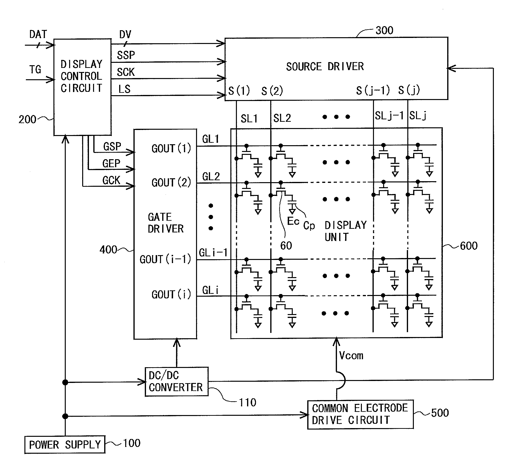
[0186]FIG. 2 is a block diagram for illustration of an overall configuration of an active matrix-type liquid crystal display device according to a first embodiment of the present invention. As illustrated in FIG. 2, this liquid crystal display device is provided with a power supply 100, a DC / DC converter 110, a display control circuit 200, a source driver (video signal line drive circuit) 300, a gate driver (scanning signal line drive circuit) 400, a common electrode drive circuit 500, and a display unit 600. Here, the gate driver 400 is formed using amorphous silicon, polycrystalline silicon, microcrystalline silicon, oxide semiconductor (e.g., IGZO), or the like on a display panel including the display unit 600. Specifically, in this embodiment, the gate driver 400 and the display unit 600 are formed on the same substrate (an array substrate that is one of two substrates that constitute a liquid crystal panel).

[0187]The dis...

second embodiment

2. Second Embodiment

2.1 Configuration of Bistable Circuit

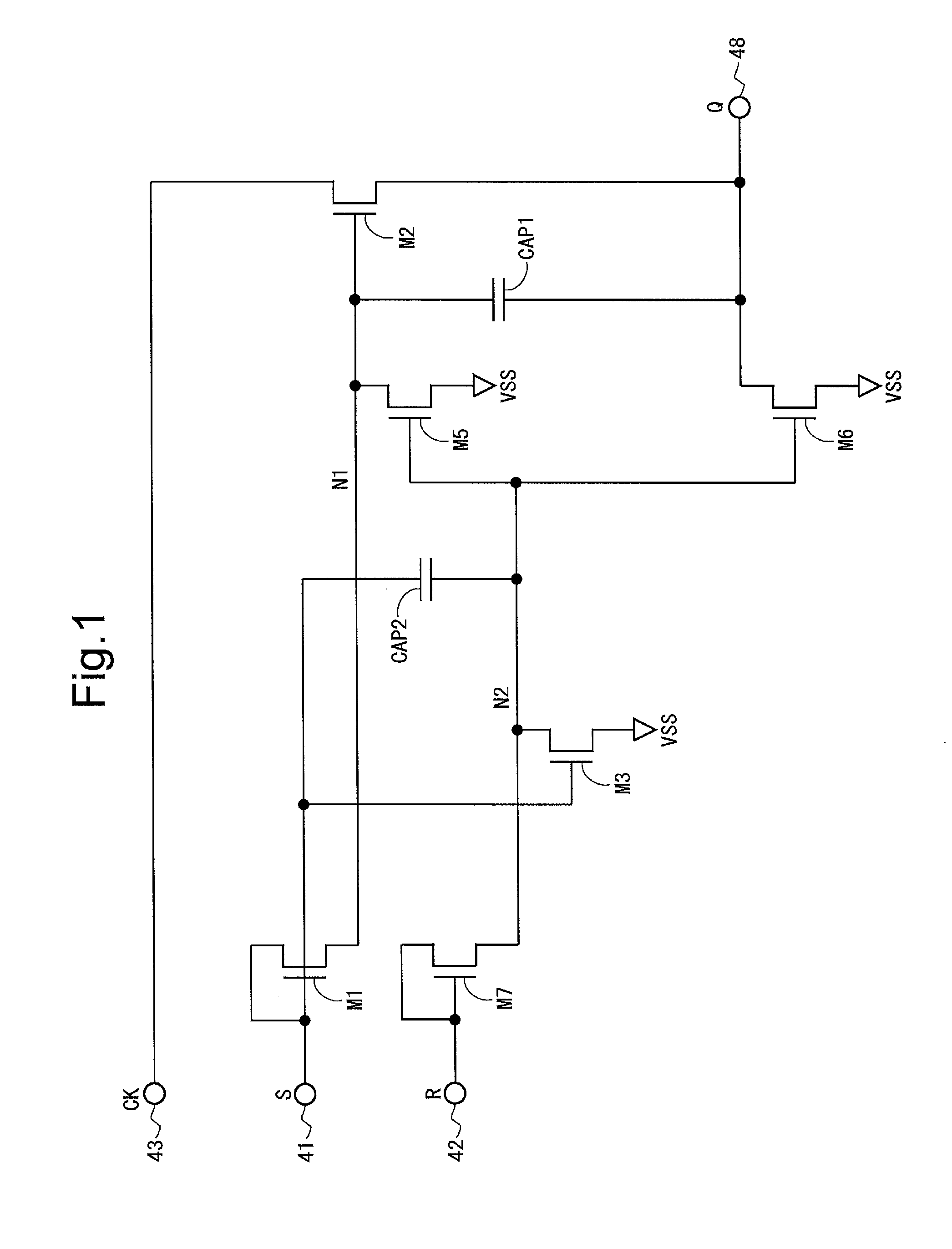
[0228]FIG. 21 is a circuit diagram showing a configuration of a bistable circuit according to a second embodiment of the present invention. Here, an overall configuration and an operation of a liquid crystal display device and a configuration and an operation of a gate driver are the same as those in the first embodiment, and therefore descriptions for these are omitted.

[0229]According to the first embodiment, for the thin-film transistor M5, the gate terminal is connected to the second-node N2, the drain terminal is connected to the first-node N1, and the source terminal is connected to the input terminal for the DC power supply potential VSS. However, the present invention is not limited to this. As illustrated in FIG. 21, the source terminal of the thin-film transistor M5 may be connected to the output terminal 48.

2.2 Effects

[0230]According to this embodiment, the source terminal of the thin-film transistor M5 is supplied w...

third embodiment

3. Third Embodiment

3.1 Configuration of Bistable Circuit

[0231]FIG. 22 is a circuit diagram showing a configuration of a bistable circuit according to a third embodiment of the present invention. Here, an overall configuration and an operation of a liquid crystal display device and a configuration and an operation of a gate driver are the same as those in the first embodiment, and therefore descriptions for these are omitted.

[0232]According to this embodiment, the bistable circuit is provided with a thin-film transistor M4, in addition to the components of the first embodiment illustrated in FIG. 1. For the thin-film transistor M4, a gate terminal is connected to the output terminal 48, a drain terminal is connected to the second-node N2, and a source terminal is connected to the input terminal for the DC power supply potential VSS. The thin-film transistor M4 functions so as to change the potential of the second-node N2 to the VSS potential when the potential of the output terminal ...


PUM


Abstract

A bistable circuit includes an input terminal (41) for a set signal, an input terminal (42) for a reset signal, an output terminal (48) for a state signal, a thin-film transistor (M2) for increasing a potential of the output terminal (48) based on a first clock, a thin-film transistor (M1) for increasing a potential of a first-node connected to a gate terminal of the thin-film transistor (M2) based on the set signal, a thin-film transistor (M5) for decreasing the potential of the first-node, a thin-film transistor (M7) for increasing a potential of a second-node connected to a gate terminal of the thin-film transistor (M5) based on the reset signal, a thin-film transistor (M6) for decreasing the potential of the output terminal (48) based on the potential of the second-node, a thin-film transistor (M3) for increasing the potential of the second-node based on the set signal, and a capacitor (CAP2) having one end connected to the second-node and the other end connected to the input terminal (41).

Description

TECHNICAL FIELD[0001]The present invention relates to a display device and a drive circuit thereof, and in particular to a scanning signal line drive circuit configured by a plurality of shift registers, that drives scanning signal lines which are arrayed in a display unit of the display device.BACKGROUND ART[0002]In recent years, in liquid crystal display devices, a gate driver (scanning signal line drive circuit) for driving gate bus lines (scanning signal lines) have become increasingly monolithic. Conventionally, a gate driver has mostly been mounted as an IC (Integrated Circuit) chip on a peripheral part of a substrate that constitutes a liquid crystal panel. However, in recent years, it has gradually become more common to provide a gate driver directly on a substrate. Such a gate driver is called a “monolithic gate driver”, for example. In a liquid crystal display device provided with a monolithic gate driver, while a thin-film transistor using amorphous silicon (a-Si) (herein...

Claims


Application Information

Patent Timeline
IPC IPC(8): G06F3/038
CPCG09G3/3677G09G2310/0283G09G2310/0286G11C19/28G11C19/184G02F1/13454G09G3/36G02F1/133G11C19/00
Inventor TAKAHASHI, YOSHIHISAIWASE, YASUAKI
Owner SHARP KK
Why Eureka
Try Eureka