
Apparatus for producing silicon carbide single crystal

a silicon carbide and single crystal technology, applied in the direction of crystal growth process, polycrystalline material growth, coating, etc., can solve the problems of large diameter of silicon carbide single crystal wafer, difficult to meet the temperature difference between the center portion and the peripheral portion of the seed crystal, and difficult to produce a large-diameter silicon carbide single crystal. , to achieve the effect of small temperature gradient, large temperature gradient, and reduced temperature gradien

Inactive Publication Date: 2012-12-27
BRIDGESTONE CORP
View PDF1 Cites 7 Cited by
  • Summary
  • Abstract
  • Description
  • Claims
  • Application Information

AI Technical Summary

Benefits of technology

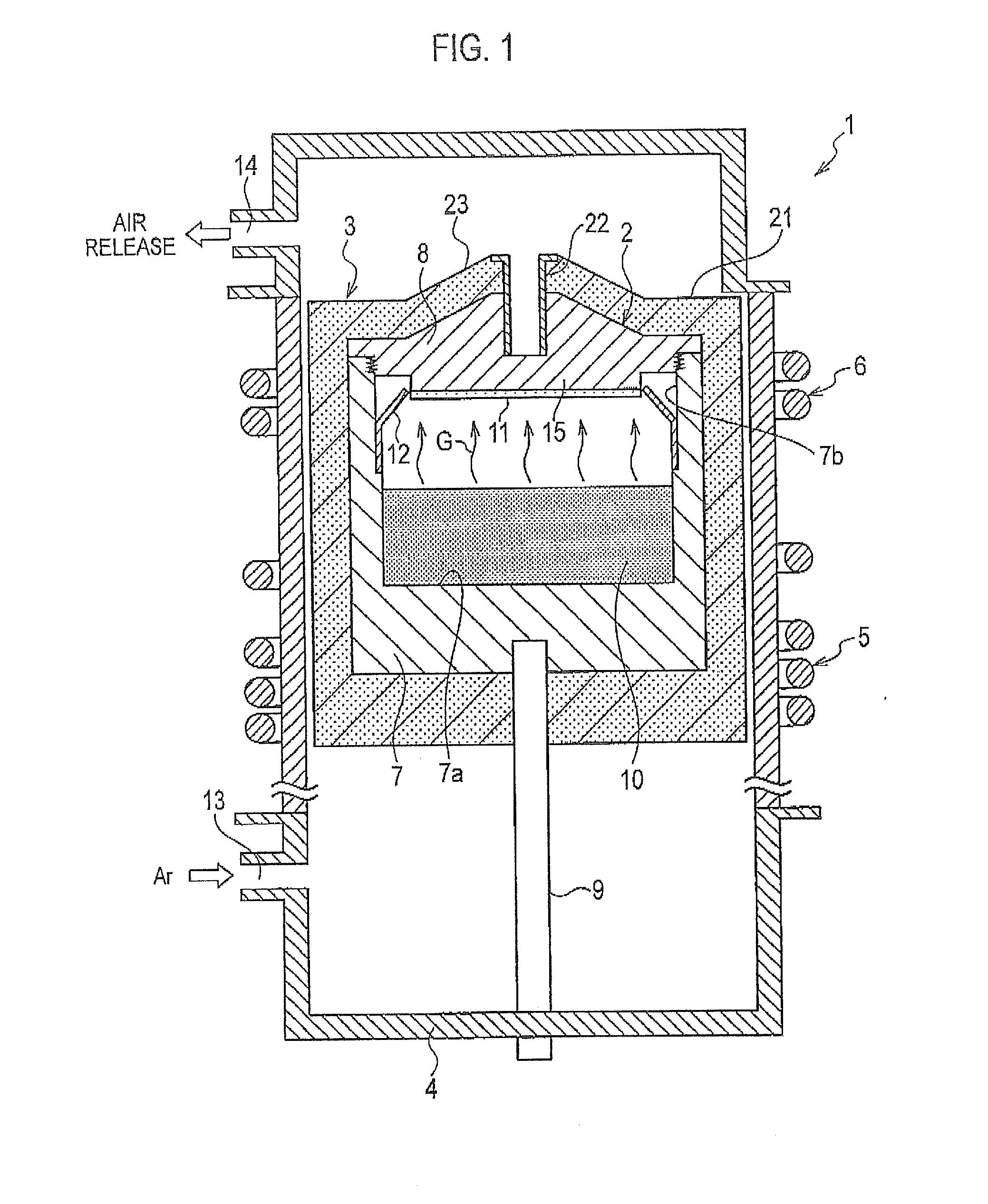
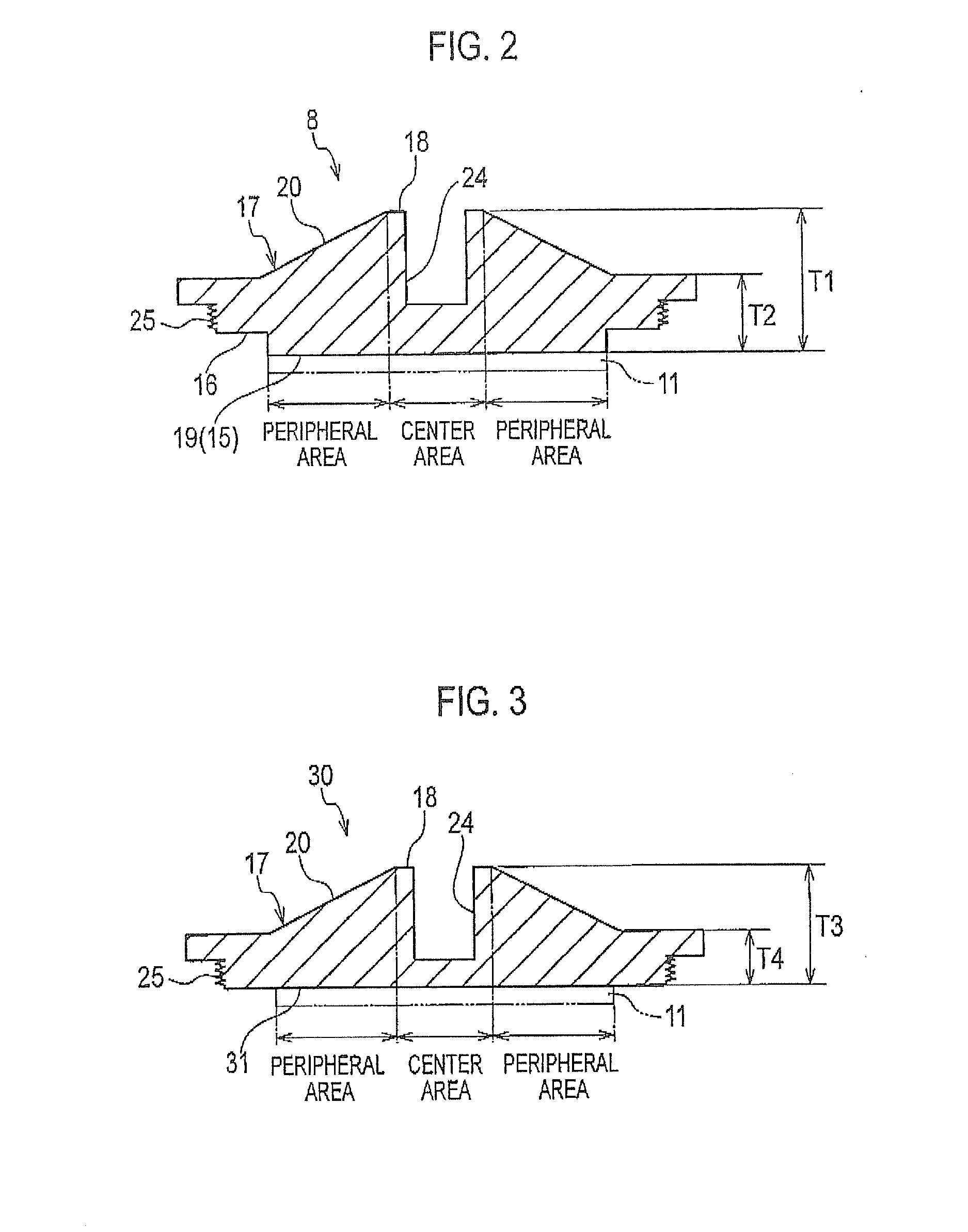
[0011]To reduce the temperature difference between the radial center and the radial outer portion of the lid 8, 30, the temperature gradient should be reduced by using a thick lid. However, in such a case, the temperature gradient at the peripheral portion of the crystal might reach or fall below the lowest value of the temperature gradient for growing a spherical single crystal. Further, it is preferable in growing crystals that the radial center portion (i.e., the center area) of the seed crystal 11 have a smaller temperature gradient than the circumferential portion (i.e., the peripheral area) thereof. For these reasons, it is the gist of the present invention that the thickness of the lid at the portion corresponding to the center area of the seed crystal is formed to be larger than the thickness of the lid at the portion corresponding to the peripheral area of the seed crystal so as to provide a small temperature gradient at the radial center portion of the lid and a large temperature gradient at the radial outer portion thereof.

Problems solved by technology

The above method, however, has a problem in giving a silicon carbide single crystal wafer a large diameter, which is demanded in recent years.
As described above, it is difficult to meet both the condition for the temperature difference between the center portion and the peripheral portion of the seed crystal and the condition for the temperature gradient, the conditions being for producing a high-quality silicon carbide single crystal.
Accordingly, it is difficult to produce a large-diameter silicon carbide single crystal using the technique disclosed in Patent Document 1.

Method used


Image

  • Apparatus for producing silicon carbide single crystal
  • Apparatus for producing silicon carbide single crystal
  • Apparatus for producing silicon carbide single crystal

Examples


Embodiment Construction

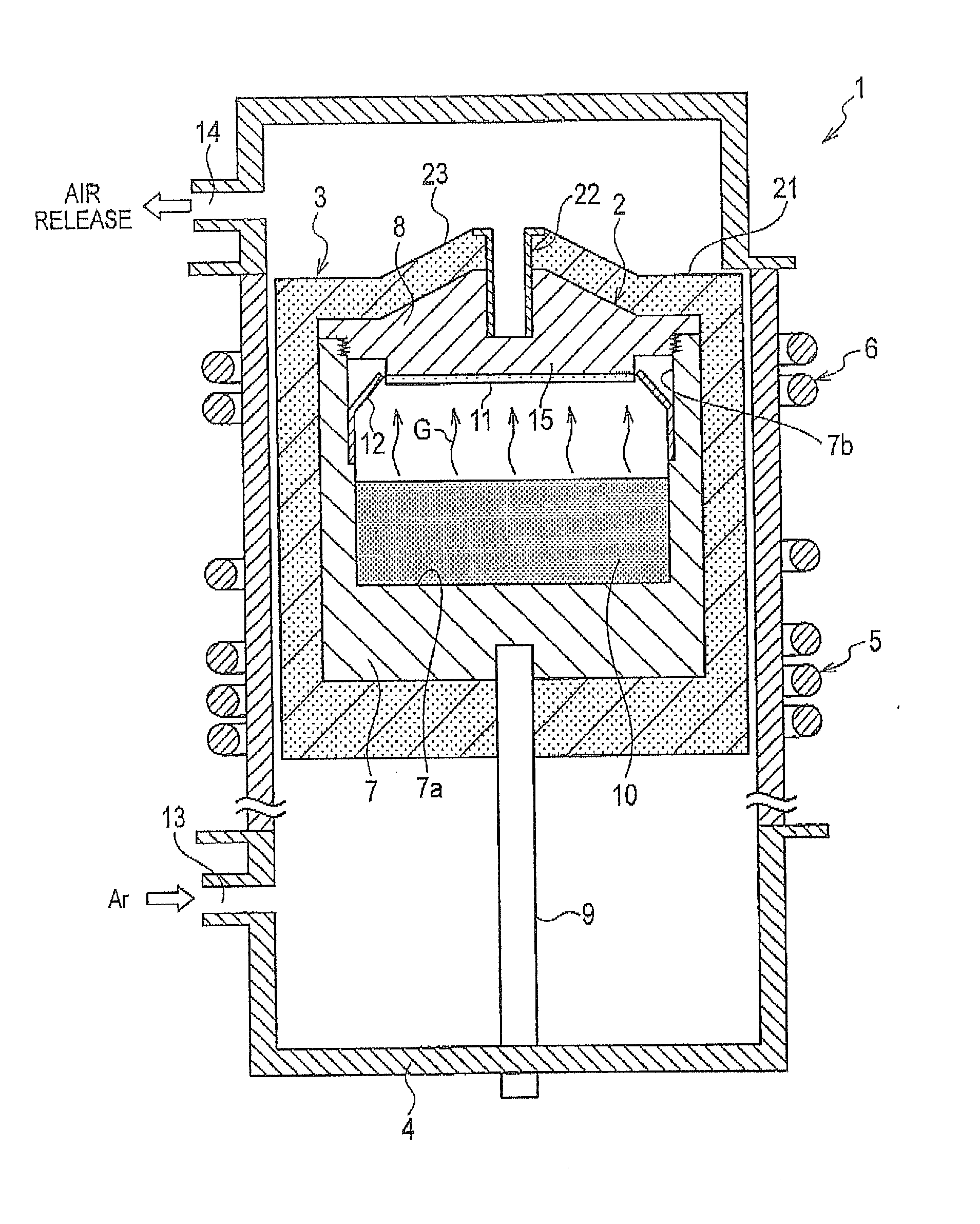
[0022]An apparatus for producing a silicon carbide single crystal according to an embodiment of the present invention will be described in detail below with reference to the drawings. Specifically, descriptions will be given as to (1) the overall configuration of the apparatus for producing a silicon carbide single crystal, (2) the detailed configurations of a lid and a heat shield, (3) a modification, (4) heat conduction in the apparatus for producing a silicon carbide single crystal according to the present invention, (5) advantageous effects, and (6) other embodiments.

[0023]Note that the drawings are only schematic, and the thicknesses of the materials and their ratios are different from the actual values. Accordingly, specific thicknesses and dimensions should be determined based on the description given below. Moreover, the drawings also include portions having different dimensional relationships and ratios from each other.

(1) Overall Configuration of Apparatus for Producing Si...


PUM

PropertyMeasurementUnit
thicknessaaaaaaaaaa
areaaaaaaaaaaa
band gapaaaaaaaaaa

Abstract

The apparatus for producing a single crystal is an apparatus for producing a silicon carbide single crystal including the crucible configured to house the seed crystal containing silicon carbide and the raw material for sublimation arranged opposite the seed crystal and used for growing the seed crystal. The crucible includes the crucible body configured to house the raw material for sublimation and the lid configured such that the seed crystal is arranged on the lid, and the thickness of the lid at the center area thereof corresponding to the radial center portion of the seed crystal is set to be larger than the thickness of the lid at the peripheral area thereof corresponding to a portion located radially outside the radial center portion of the seed crystal.

Description

TECHNICAL FIELD[0001]The present invention relates to an apparatus for producing silicon carbide single crystal for producing a silicon carbide single crystal using the improved Rayleigh method (sublimation method)BACKGROUND ART[0002]Compared to silicon, silicon carbide has a large band gap and is excellent in its breakdown characteristic, resistance to heat, and resistance to radiation. For these reasons, silicon carbide has been drawing attention as a material for electronic devices such as a small-sized semiconductor wafer with high output and for optical devices such as a light-emitting diode. In the fields of such electronic devices and optical devices, there are demands for a high-quality silicon carbide single crystal having fewer defects such as an interfusion of polycrystal and polymorphism, and pipe-shaped crystal defects (so-called micro-pipes).[0003]To answer such demands, a method has been disclosed in which a silicon carbide single crystal is grown while keeping its en...

Claims


Application Information

Patent Timeline
Patent Type & Authority Applications(United States)
IPC IPC(8): C30B23/02
CPCC30B29/36C30B23/00C30B23/06
Inventor SEKI, WATARUKONDO, DAISUKE
Owner BRIDGESTONE CORP
Learn More