Conductive film and method for its production

a technology of conductive film and conductive layer, which is applied in the direction of conductive layer on the insulating support, cell components, metal/alloy conductors, etc., can solve the problems of affecting production cost and productivity, high equipment investment, and high vacuum apparatus investment, etc., to achieve excellent transparency and conductivity, high industrial value, and simple process

Inactive Publication Date: 2012-12-27
KYOTO UNIV +2
View PDF2 Cites 10 Cited by
  • Summary
  • Abstract
  • Description
  • Claims
  • Application Information

AI Technical Summary

Benefits of technology

[0024]The production method of the invention is a method that allows large-area formation of conductive films with excellent transparency and conductivity by a simple process, and therefo...

Problems solved by technology

ITO films are produced by gas phase methods such as sputtering or vacuum vapor deposition, but gas phase methods require high vacuum apparatuses and large equipment investment.
The equipment investment and maintenance cost becomes particularly immense for purposes that require large-sized areas.
Furthermore, since the component gas pressure in the production apparatus must be precisely controlled for production of each ITO film, this affects the production cost and productivity.
However, ITO films are associated with numerous problems that must be overcome, such as the high cost of indium, difficulty of increasing conductivity while maintaining transparency, and susceptibility to bending.
In printing methods, however, productivity is reduced due to clogging of the mesh or nozzle, and it is difficult to form intricate patterns with line widths of less than 6 μm.
P...

Method used


Image

  • Conductive film and method for its production
  • Conductive film and method for its production
  • Conductive film and method for its production

Examples


examples

[0184]The invention will now be described in greater detail by examples, with the understanding that the invention is not limited to these examples.

[0185]An optical microscope (BX51123 MDS™ microscope system by Olympus Corp.) was used to observe the conductive film, and the line widths and opening widths were measured from the image at 5 locations, recording the average values as the line width and opening width.

[0186]A haze meter (NDH200™ by Nippon Denshoku Industries Co., Ltd.) was used to measure the light transmittance of the sample at 5 locations, and the average value was recorded as the transparency (light transmittance).

[0187]A serial four-point probe was mounted on a resistivity meter (LORESTA GP™ by Mitsubishi Chemical Corp.), and the surface resistance value of the sample was measured at 5 locations, recording the average value as the conductivity (surface resistance value).

[0188]Each sample was mixed in the proportion shown below to prepare monomer composition (X).

[0189]...

examples 1 to 11

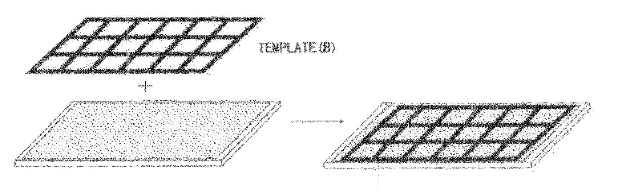
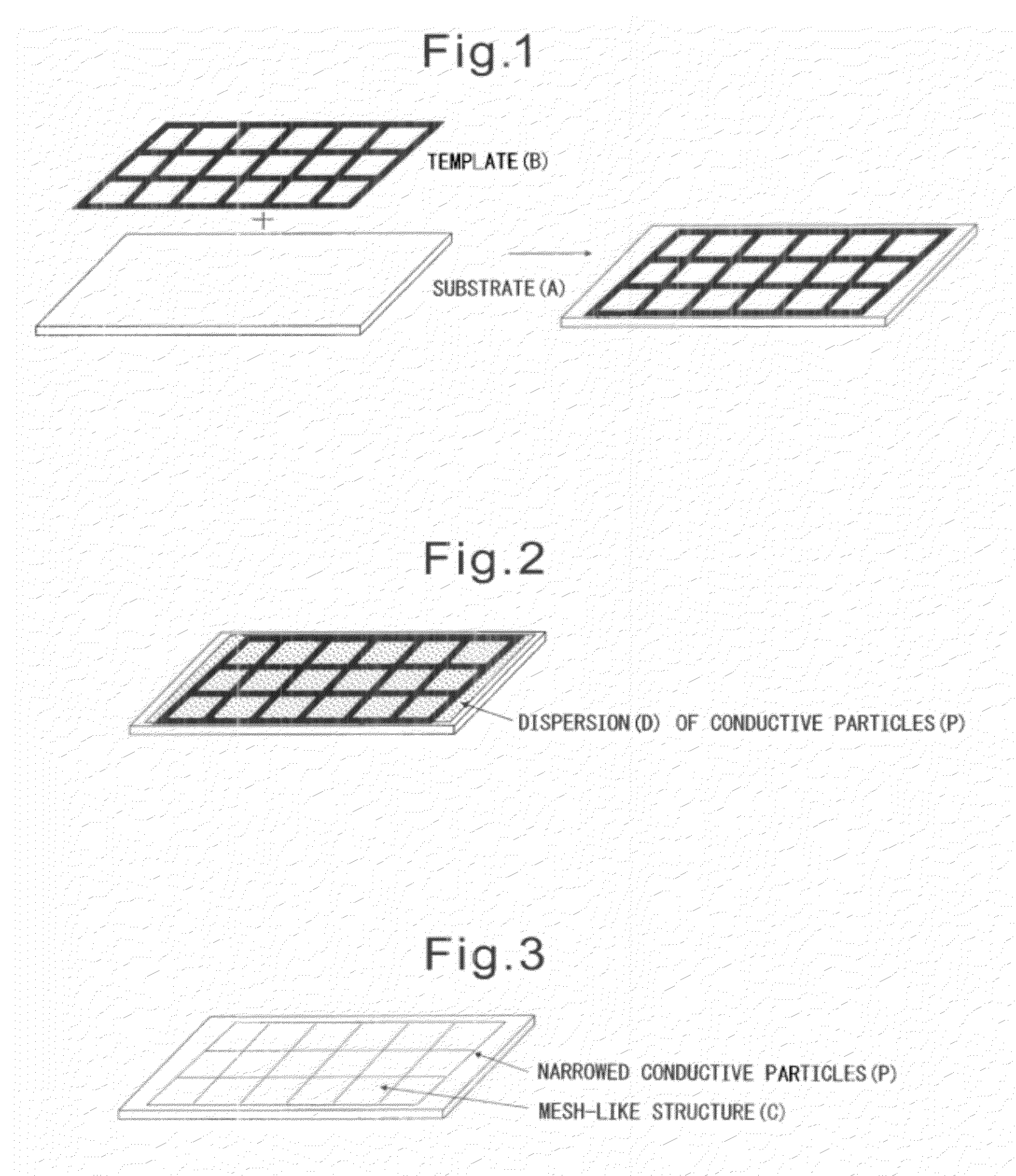
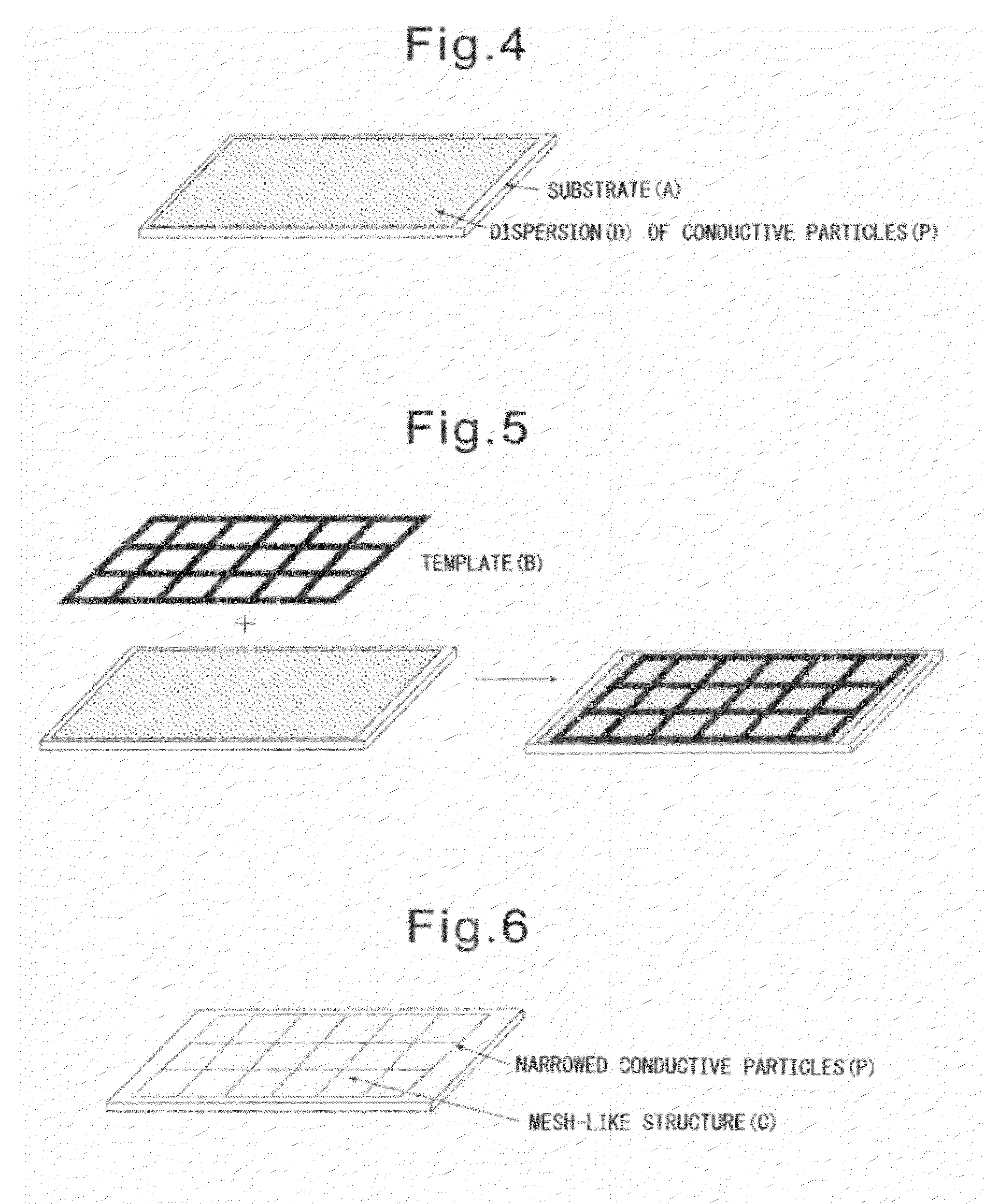
[0196]The substrate (A) used was a glass board (dimensions: 50 mm×50 mm×1.0 mm, light transmittance: 91%, surface resistance value: ≧1010Ω / sq., product of Matsunami Glass Industries, Ltd.).

[0197]The template (B) used was a stainless steel wire mesh (plain weave wire mesh), shown in Table 1.

[0198]The dispersion (D) used was an aqueous dispersion of gold fine particles, appropriately diluted with deionized water to the solid content listed in Table 1.

[0199]FINESPHERE GOLD W011 (product of Nippon Paint Co., Ltd., conductive fine particles: gold, weight-average particle size: 10 nm, solid content: 10 mass %, trade name)

[0200]FINESPHERE GOLD W101 (product of Nippon Paint Co., Ltd., conductive fine particles: gold, weight-average particle size: 20 nm, solid content: 10 mass %, trade name)

[0201]A stainless steel wire mesh was placed on the surface of a glass board, and the aqueous dispersion of gold fine particles in the coating amount listed in Table 1 was developed and allowed to stand a...

example 12

[0207]A conductive film was obtained in the same manner as Example 5, except that after drying the aqueous dispersion of gold fine particles at 5° C. for 60 minutes, the same procedure was repeated (development-drying, twice).


PUM

PropertyMeasurementUnit
Lengthaaaaaaaaaa
Fractionaaaaaaaaaa
Massaaaaaaaaaa

Abstract

To provide a method for producing a conductive film with excellent transparency and conductivity by a simple method suitable for large-area production.
A method for producing a conductive film comprising a step of placing a template (B), having openings in a mesh structure running from the side that is to contact a substrate (A) through to the back side, on the surface of the substrate (A), and spreading a dispersion (D) of conductive particles (P) on the surface of the substrate (A) on which the template (B) has been placed, and drying it, thereby forming a mesh-like structure (C) of the conductive particles (P) near the points of contact between the substrate (A) and the template (B), and then removing the template (B) from the substrate (A) to form a mesh-like structure (C) of the conductive particles (P) on the surface of the substrate (A).

Description

TECHNICAL FIELD[0001]The present invention relates to a conductive film with excellent transparency and conductivity, and to a method for its production.BACKGROUND ART[0002]Conductive films with excellent transparency are widely used for such purposes as display electrodes for flat panel displays such as plasma displays and liquid crystal displays; transparent electrodes for touch panels; transparent electrodes for solar cells; and electromagnetic wave shielding films.[0003]Tin-doped indium oxide (Indium Tin Oxide, hereunder referred to as “ITO”) is well known as a material for forming conductive films with excellent transparency. ITO films are produced by gas phase methods such as sputtering or vacuum vapor deposition, but gas phase methods require high vacuum apparatuses and large equipment investment. The equipment investment and maintenance cost becomes particularly immense for purposes that require large-sized areas. Furthermore, since the component gas pressure in the producti...

Claims


Application Information

Patent Timeline
IPC IPC(8): H05K1/02C25D15/00B05D5/12
CPCH01B1/02H05K9/0094H05K1/097H05K3/1216H01B5/14H01B13/00H05K1/092
Inventor HIGASHITANI, KOTSUDO, YASUHIRONAKAYAMA, MASAKIKAKE, SHINJI
Owner KYOTO UNIV
Why Eureka
Try Eureka