Semiconductor device and manufacturing method thereof

Active Publication Date: 2013-01-10
SEMICON ENERGY LAB CO LTD
View PDF3 Cites 119 Cited by
  • Summary
  • Abstract
  • Description
  • Claims
  • Application Information

AI Technical Summary

Benefits of technology

[0008]An improvement in the on-state characteristics (e.g., on-state current and field-effect mobility) of a transistor leads to high-speed response to an input signal and high-speed operation of a semiconductor device; thus, a semiconductor device with higher performance can be achieved. Meanwhile it is necessary t

Problems solved by technology

If the threshold voltage value is negative even while the field-effect mobility is high, it is difficult to control the circuit.
Such a transistor in which a cha

Method used


Image

  • Semiconductor device and manufacturing method thereof
  • Semiconductor device and manufacturing method thereof
  • Semiconductor device and manufacturing method thereof

Examples


embodiment 1

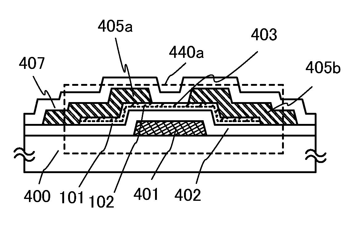
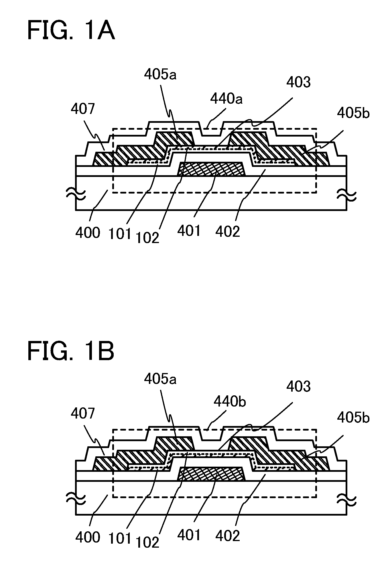
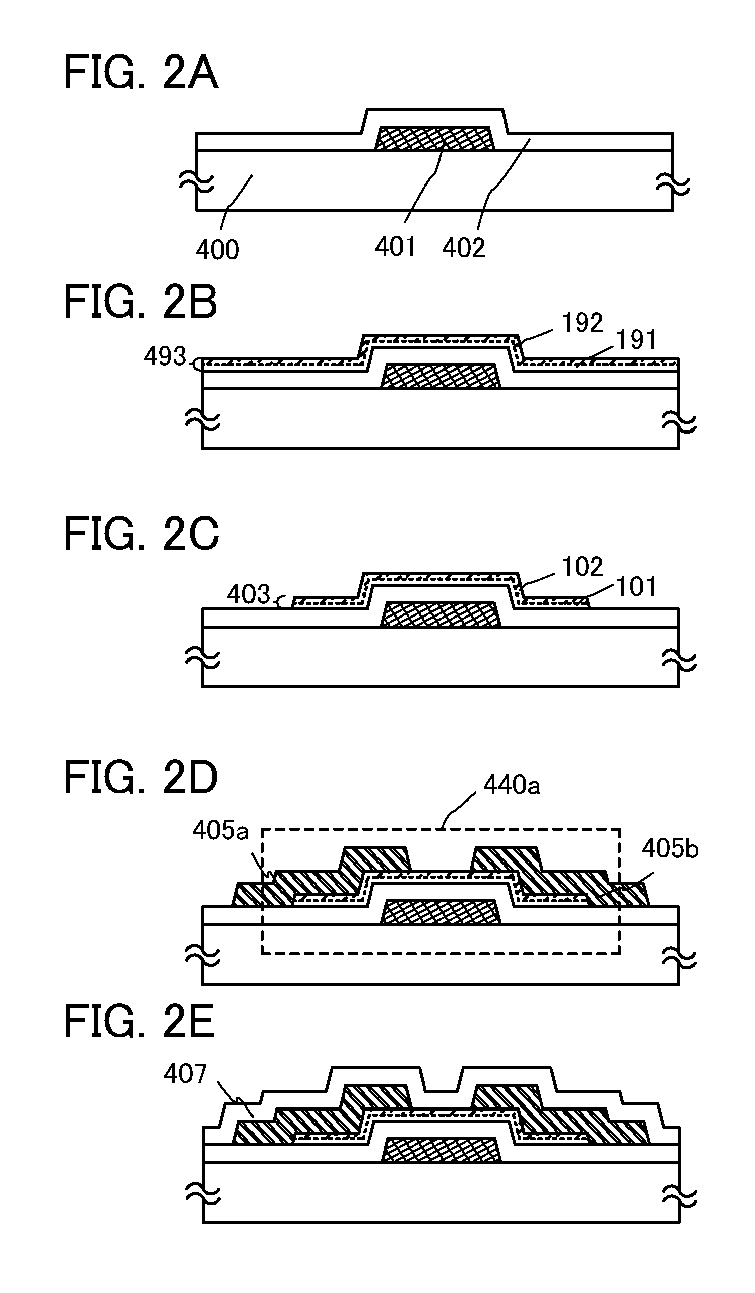
[0075]In this embodiment, an embodiment of a semiconductor device and a method for manufacturing the semiconductor device is described with reference to FIGS. 1A and 1B and FIGS. 3A to 3C. In this embodiment, a transistor including an oxide semiconductor film is described as an example of the semiconductor device.

[0076]The transistor may have a single-gate structure in which one channel formation region is formed, a double-gate structure in which two channel formation regions are formed, or a triple-gate structure in which three channel formation regions are formed. Alternatively, the transistor may have a dual-gate structure including two gate electrode layers positioned over and under a channel formation region with a gate insulating film provided therebetween.

[0077]A transistor 440a shown in FIG. 1A and a transistor 440b shown in FIG. 1B are examples of an inverted staggered, bottom-gate transistor.

[0078]As shown in FIGS. 1A and 1B, each of the transistors 440a and 440b include a...

embodiment 2

[0219]In this embodiment, another embodiment of a semiconductor device and a method for manufacturing the semiconductor device is described with reference to FIGS. 7A to 7D, FIGS. 8A to 8D, and FIGS. 11A and 11B. The above embodiment can be applied to the same portion as, a portion having a function similar to, or a step similar to that in the above embodiment; thus, repetitive description is omitted. In addition, detailed description of the same portions is also omitted.

[0220]Described in this embodiment is an example in which an upper oxide semiconductor layer covers the side surface of a lower oxide semiconductor layer in the oxide semiconductor stacked layer.

[0221]A transistor 340 shown in FIGS. 7A to 7C is an example of an inverted staggered, bottom-gate transistor. FIG. 7A is a plane view; FIG. 7B is a cross-sectional diagram along dashed line X-Y in FIG. 7A; FIG. 7C is a cross-sectional diagram along dashed line V-W in FIG. 7A.

[0222]As shown in FIG. 7B, which is the cross-sec...

embodiment 3

[0250]In this embodiment, another embodiment of a semiconductor device and a method for manufacturing the semiconductor device is described with reference to FIGS. 5A to 5D. The above embodiment can be applied to the same portion as, a portion having a function similar to, or a step similar to that in the above embodiment; thus, repetitive description is omitted. In addition, detailed description of the same portions is also omitted.

[0251]Described in this embodiment is an example in which in a method for manufacturing a semiconductor device according to one embodiment of the present invention, oxygen (which includes at least one of an oxygen radical, an oxygen atom, and an oxygen ion) is added to the oxide semiconductor stacked layer to supply oxygen to the film after the oxide semiconductor stacked layer is dehydrated or dehydrogenated.

[0252]The dehydration or dehydrogenation treatment may accompany elimination of oxygen which is a main constituent material of an oxide semiconduct...


PUM


Abstract

Provided are a transistor which has electrical characteristics requisite for its purpose and uses an oxide semiconductor layer and a semiconductor device including the transistor. In the bottom-gate transistor in which at least a gate electrode layer, a gate insulating film, and the semiconductor layer are stacked in this order, an oxide semiconductor stacked layer including at least two oxide semiconductor layers whose energy gaps are different from each other is used as the semiconductor layer. Oxygen and/or a dopant may be added to the oxide semiconductor stacked layer.

Description

BACKGROUND OF THE INVENTION[0001]1. Field of the Invention[0002]The present invention relates to a semiconductor device and a method for manufacturing the semiconductor device.[0003]In this specification, the semiconductor device generally means any device which can function by utilizing semiconductor characteristics, and an electrooptic device, a semiconductor circuit, and electronic equipment are all included in the category of the semiconductor device.[0004]2. Description of the Related Art[0005]Attention has been focused on a technique for forming a transistor with use of a semiconductor thin film formed over a substrate having an insulating surface (the transistor also referred to as a thin film transistor (TFT)). The transistor has been applied to a wide range of electronic devices such as an integrated circuit (IC) or an image display device (display device). A silicon semiconductor material is widely known as a material for a semiconductor thin film applicable to a transisto...

Claims


Application Information

Patent Timeline
IPC IPC(8): H01L29/78H01L21/336H05B44/00
CPCH01L29/78696H01L29/7869H01L29/045H01L29/66742H01L29/786H01L29/78693H01L27/1225H01L27/1229H10K59/1216H10K59/1213H01L29/24
Inventor YAMAZAKI, SHUNPEISHINOHARA, SATOSHI
Owner SEMICON ENERGY LAB CO LTD
Why Eureka
Try Eureka