Epitaxial wafer including nitride-based semiconductor layers

a technology of nitride-based semiconductor layers and epitaxial wafers, which is applied in the field of epitaxial wafers, can solve the problems of difficult control of the warpage of the gan substrate, the edge dislocation density is still greater than about 110sup>10 /sup>cmsup>2, and achieve the effect of improving the warpage and crystallinity of the epitaxial wafer

Inactive Publication Date: 2013-01-24
SHARP KK
View PDF4 Cites 31 Cited by
  • Summary
  • Abstract
  • Description
  • Claims
  • Application Information

AI Technical Summary

Benefits of technology

[0015]In view of the problems as described above, a main object of the present invention is to improve the warpage and crystallinity of the epitaxial wafer usable for the hetero-junction field effect type transistor.

Problems solved by technology

In the case of producing an epitaxial wafer including a hetero-junction interface formed by a GaN channel layer and an AlGaN barrier layer usable for a hetero-junction field effect type transistor for example, the nitride semiconductor layers have conventionally been crystal-grown on a substrate of a different kind of material such as sapphire, Si or the like, because a GaN substrate is expensive.
Regarding the multilayered buffer layer structure, in the case that the repetition number of constituent layers therein is increased and the total thickness from the upper surface of the GaN channel layer thereon to the upper surface of the substrate is increased, there is a problem that the wafer shows a warpage of not a simple parabolic shape but an M-shape as shown in a graph of FIG. 2 and it becomes difficult to control the warpage of the wafer.
As seen in FIG. 3, while the density of edge dislocations included in the GaN channel layer on the multilayered buffer layer structure decreases as the thickness of the buffer layer structure increases, there is a problem that the edge dislocation density is still greater than about 1×1010 cm−2 even when the total thickness is about 5 μm.
However, there is a problem that the warpage of the wafer is increased and cracks are generated when the thickness of the composition-gradient buffer layer structure is increased.
Further, even with structures in which the multilayered buffer structure and the composition-gradient buffer structure are combined, there is a problem that in some cases the effect of improving the crystallinity is not realized at all depending on how the multilayered buffer layer structure and the composition-gradient buffer layer structure are combined.

Method used


Image

  • Epitaxial wafer including nitride-based semiconductor layers
  • Epitaxial wafer including nitride-based semiconductor layers
  • Epitaxial wafer including nitride-based semiconductor layers

Examples


example 1

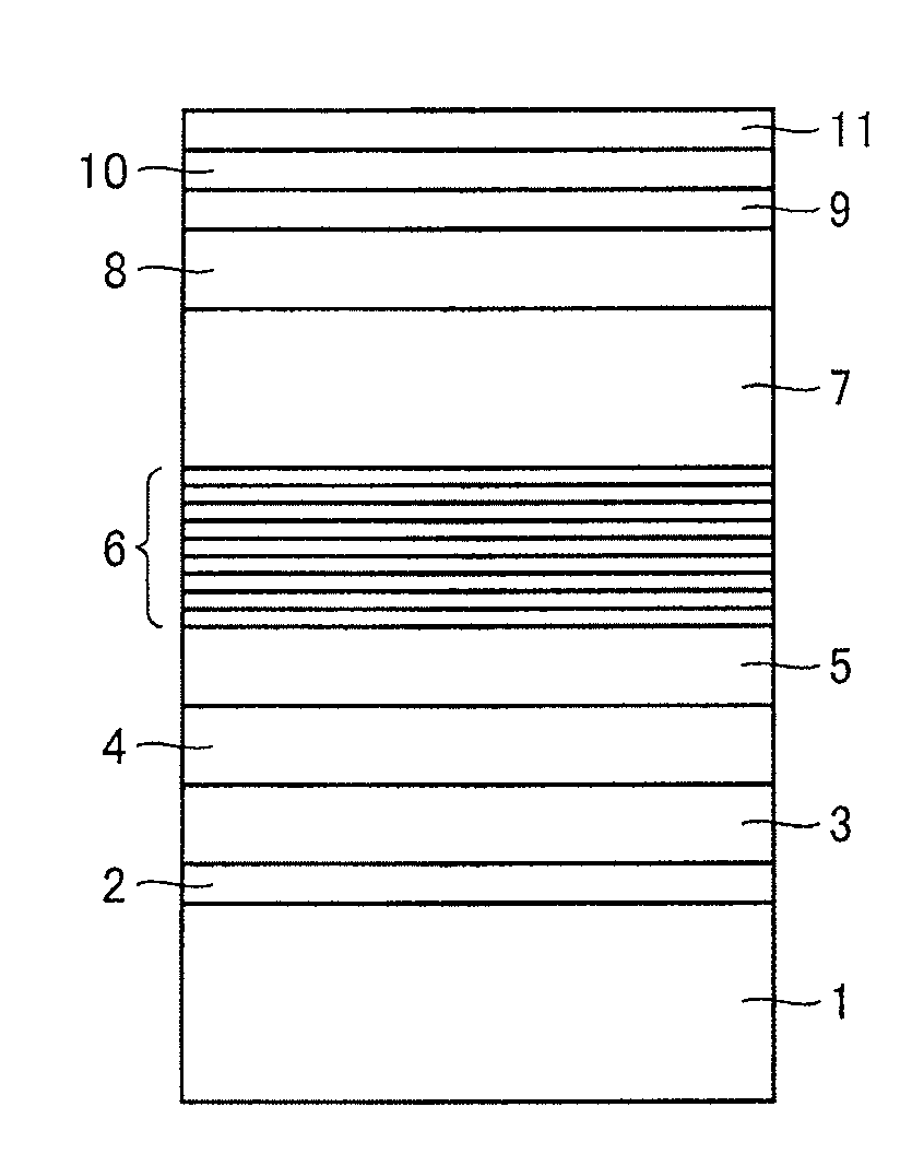
[0040]FIG. 1 is a schematic cross-sectional view illustrating an epitaxial wafer for a hetero-junction field effect type transistor, according to Example 1 of the present invention.

[0041]In production of this wafer, a Si substrate 1 of a 4-inch diameter is used as a substrate. Prior to crystal growth of nitride-based semiconductor layers, the surface oxide film of Si substrate 1 is removed by hydrofluoric acid type etchant and then the substrate is set in a chamber of a MOCVD (metal organic chemical vapor deposition) apparatus.

[0042]In the MOCVD apparatus, the substrate is heated to 1100° C. and the substrate surface is cleaned in a hydrogen atmosphere at a chamber pressure of 13.3 kPa.

[0043]Then while the substrate temperature and the chamber pressure are maintained, the Si substrate surface is nitrided by letting ammonia NH3 (12.5 slm) flow. Subsequently an AlN layer 2 is deposited to a thickness of 200 nm under the conditions of a TMA (trimethylaluminum) flow rate of 117 μmol / min...


PUM


Abstract

An epitaxial wafer including nitride-based semiconductor layers usable for a hetero-junction field effect type transistor, includes a first buffer layer of AlN or AlON, a second buffer layer of AlxGa1-xN having its Al composition ratios decreased in a stepwise fashion, a third buffer layer including a multilayer of repeatedly stacked AlaGa1-aN layers/AlbGa1-bN layers disposed on the second buffer layer, a GaN channel layer, and an electron supply layer in this order on a Si substrate, wherein the Al composition ratio x in the uppermost part of the second buffer layer is in a range of 0≦x≦0.3.

Description

[0001]This nonprovisional application is based on Japanese Patent Application No. 2011-157849 filed on Jul. 19, 2011 with the Japan Patent Office, the entire contents of which are hereby incorporated by reference.BACKGROUND OF THE INVENTION[0002]1. Field of the Invention[0003]The present invention is related to an epitaxial wafer including a plurality of layers of nitride-based semiconductors belonging to III-V group compound semiconductors and particularly to improvement in warpage and crystallinity of the epitaxial wafer usable for a hetero-junction field effect type transistor. Incidentally it is known that two-dimensional electron gas can be generated at a hetero-junction interface in such a nitride-based semiconductor epitaxial wafer.[0004]2. Description of the Background Art[0005]In the case of producing an epitaxial wafer including a hetero-junction interface formed by a GaN channel layer and an AlGaN barrier layer usable for a hetero-junction field effect type transistor for...

Claims


Application Information

Patent Timeline
Patent Type & Authority Applications(United States)
IPC IPC(8): H01L29/20
CPCH01L21/02381H01L21/02458H01L21/02488H01L21/02507H01L29/207H01L21/0262H01L29/66462H01L29/7787H01L29/2003H01L21/0254
Inventor TERAGUCHI, NOBUAKIHONDA, DAISUKEITO, NOBUYUKIYAGURA, MOTOJI
Owner SHARP KK
Why Eureka
Try Eureka