Tensile strained semiconductor photon emission and detection devices and integrated photonics system

a technology of semiconductor photon emission and detection device, applied in the field of optical systems, can solve the problems of low efficiency of light emission using the raman effect, difficult on-chip light emission, and inefficient materials for ligh

Active Publication Date: 2013-02-14
ACORN SEMI LLC
View PDF3 Cites 58 Cited by
  • Summary
  • Abstract
  • Description
  • Claims
  • Application Information

AI Technical Summary

Problems solved by technology

Conventionally these are not efficient materials for light emission because the conduction band involved in a direct optical transition is not occupied, so that there are essentially no electron-hole pairs that can recombine and generate a photon directly, without the additional contribution of another entity such as a lattice vibration or impurity.
On-chip light emission is very challenging when using group IV semiconductors as the optically active, light-emitting material in the optical layer.
Light emission using the Raman effect is a low efficiency process.
Current optical components for light sources, modulators or even detectors cannot operate at these frequencies.

Method used


Image

  • Tensile strained semiconductor photon emission and detection devices and integrated photonics system
  • Tensile strained semiconductor photon emission and detection devices and integrated photonics system
  • Tensile strained semiconductor photon emission and detection devices and integrated photonics system

Examples


Embodiment Construction

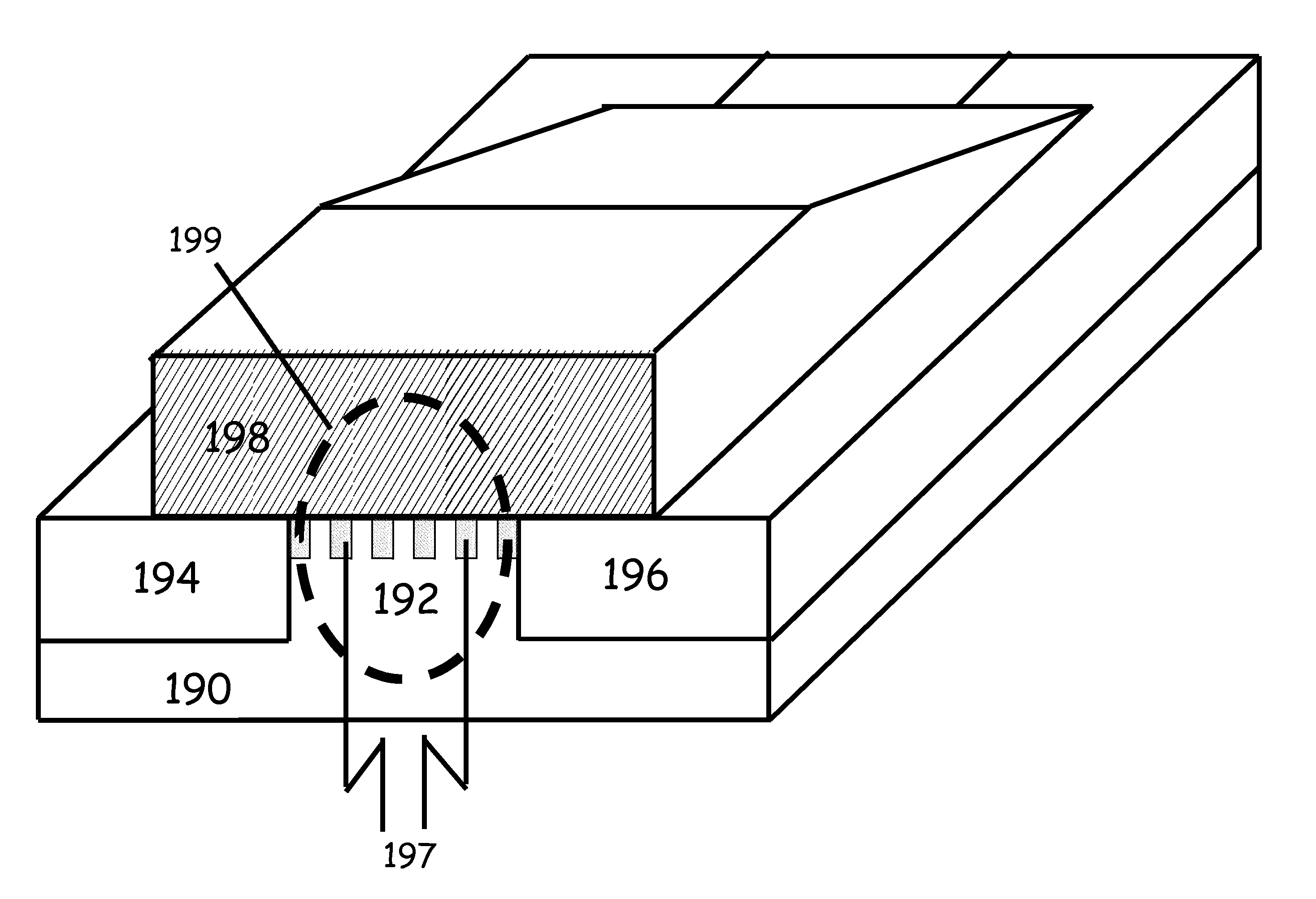
[0017]An aspect of the present invention provides an optical device having a germanium region in contact with a plurality of stressor regions. The plurality of stressor regions induces tensile strain within the germanium region. The tensile strain in at least a portion of the germanium region is sufficient to cause a portion of the germanium region to have a direct band gap. A junction is positioned in or adjacent the portion of the germanium region, the junction having a first side with a first majority carrier type and a second side with a second majority carrier type. First and second contacts are respectively coupled to the first side of the junction and the second side of the junction.

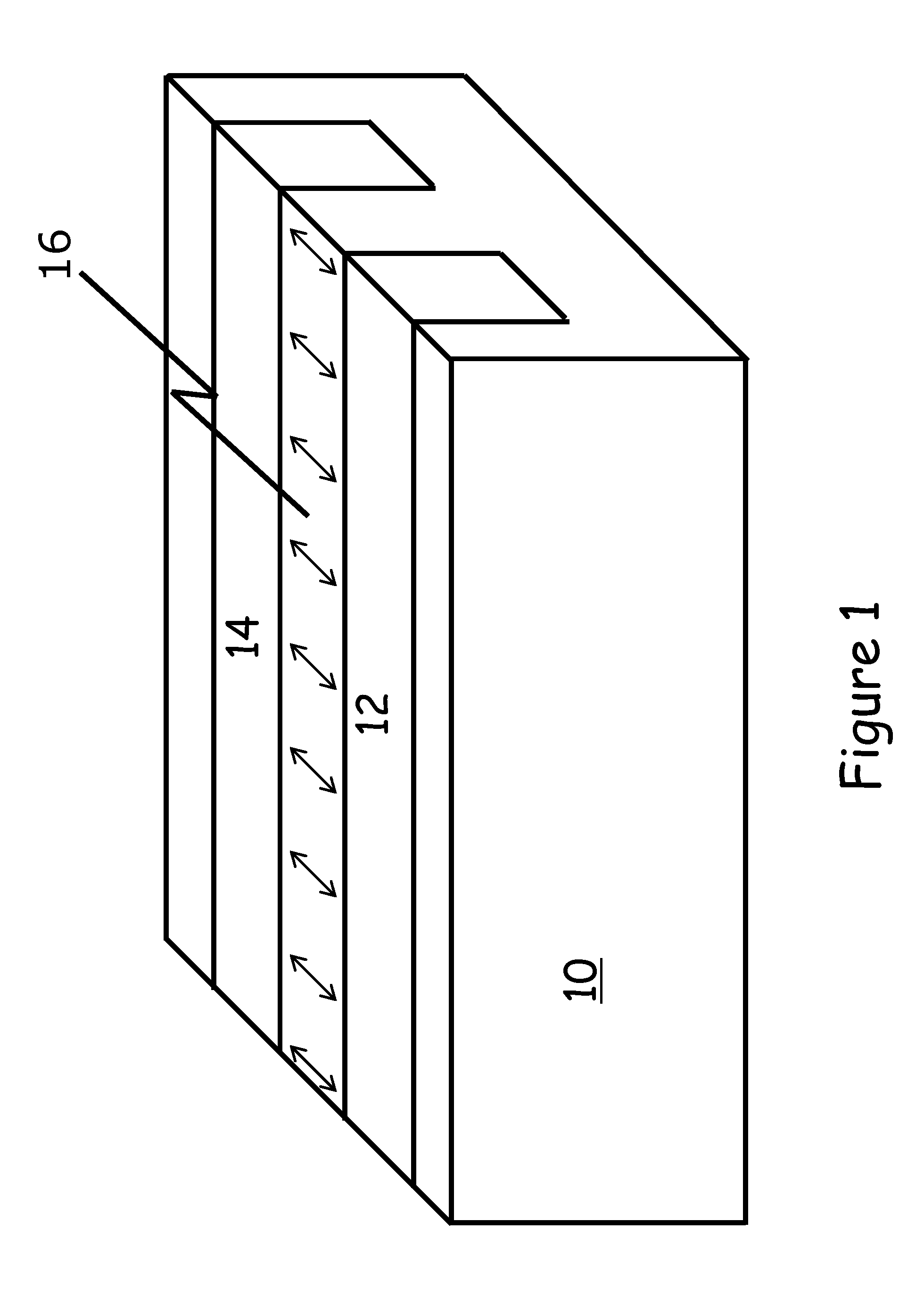
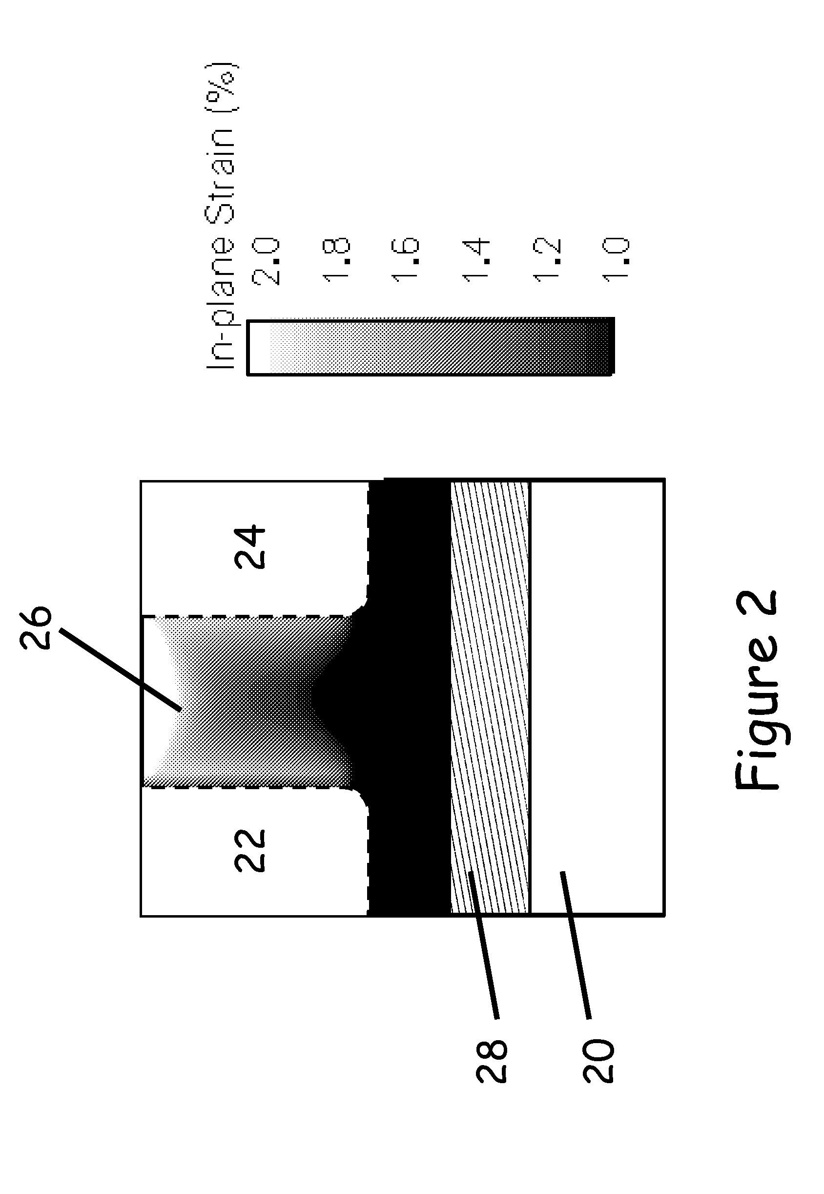
[0018]According to another aspect of the present invention, an optical device comprises first and second germanium regions. The first germanium region is in contact with a first tensile stressor so that the first germanium region has biaxial tensile strain in at least a first portion of the first ...


PUM

PropertyMeasurementUnit
thicknessaaaaaaaaaa
thicknessaaaaaaaaaa
widthaaaaaaaaaa

Abstract

Tensile strained germanium is provided that can be sufficiently strained to provide a nearly direct band gap material or a direct band gap material. Compressively stressed or tensile stressed stressor materials in contact with germanium regions induce uniaxial or biaxial tensile strain in the germanium regions. Stressor materials may include silicon nitride or silicon germanium. The resulting strained germanium structure can be used to emit or detect photons including, for example, generating photons within a resonant cavity to provide a laser.

Description

1. FIELD OF THE INVENTION[0001]The present invention relates generally to optical systems that include semiconductor light emitting devices or semiconductor light detectors. More specifically, the present invention relates to semiconductor light emitting or detecting devices that incorporate a strained group IV semiconductor material in an active region.2. DESCRIPTION OF THE RELATED ART[0002]There is continuing interest in using group IV semiconductor materials in photonics systems because of the ease of manufacturing such systems and the ease of integrating these group IV photonics with circuitry. Silicon, germanium and their alloy are the group IV semiconductors most frequently considered for photonics systems. For example, light emission from silicon or within silicon is of great interest. Silicon and germanium exhibit an indirect bandgap, as does their alloy over its full range of compositions. Conventionally these are not efficient materials for light emission because the condu...

Claims


Application Information

Patent Timeline
Patent Type & Authority Applications(United States)
IPC IPC(8): H04B10/12H01L31/18H01S5/32H01L33/34H01L33/14H01L31/109
CPCH01L31/0352H01S5/2203H01S5/227H01S5/3201H01S5/3223H01S5/187B82Y20/00H01L31/028H01L31/1808Y02E10/547H01S5/125H01L33/34H01L27/14625H01L27/14643H01L27/14H01S5/3224H01S5/3427
Inventor CLIFTON, PAUL A.GOEBEL, ANDREASGAINES, R. STOCKTON
Owner ACORN SEMI LLC
Why Eureka
Try Eureka