

Semiconductor device
a semiconductor film and semiconductor technology, applied in semiconductor devices, instruments, electrical equipment, etc., can solve problems such as adverse effects on transistor characteristics, and achieve the effect of improving the crystallinity of oxide semiconductor films and stable electric characteristics
- Summary
- Abstract
- Description
- Claims
- Application Information
AI Technical Summary
Benefits of technology
Problems solved by technology
Method used
Image

Examples
embodiment 1
[0055]In this embodiment, one embodiment of a semiconductor device and a manufacturing method thereof will be described with reference to FIGS. 1A and 1B, FIGS. 2A and 2B, FIGS. 3A and 3B, FIGS. 4A to 4E, and FIGS. 5A to 5E.
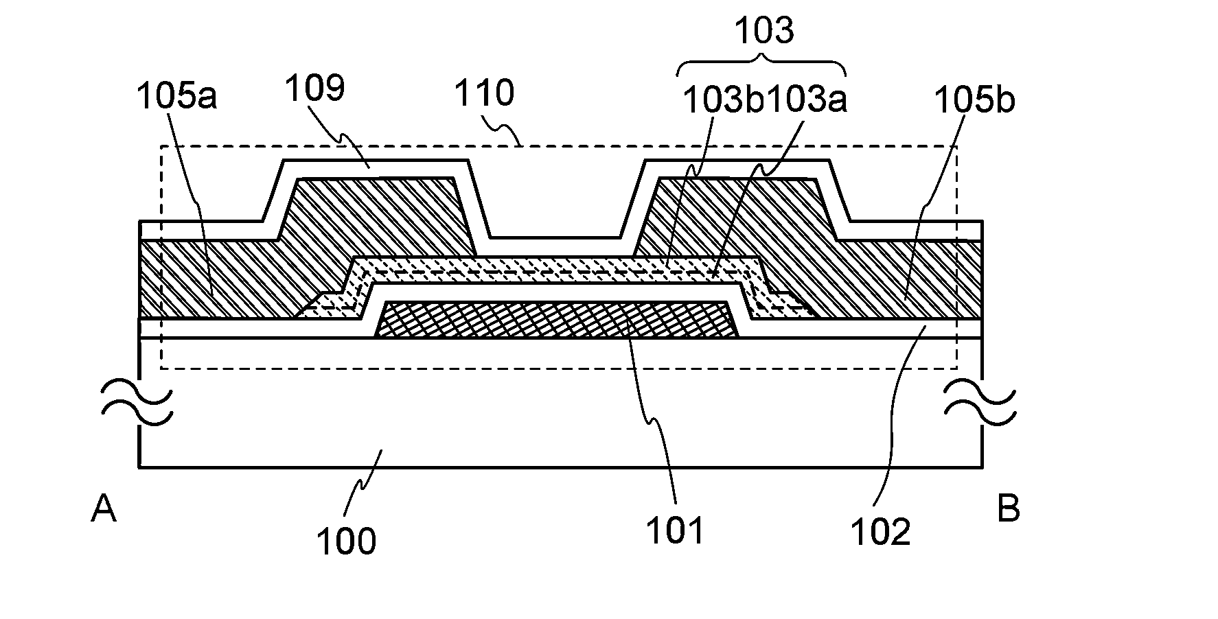
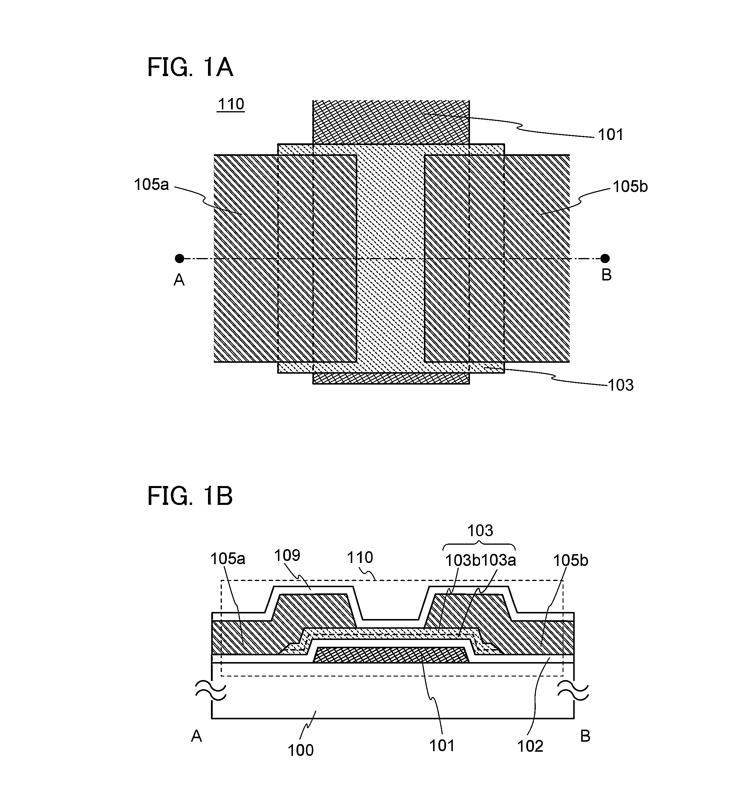
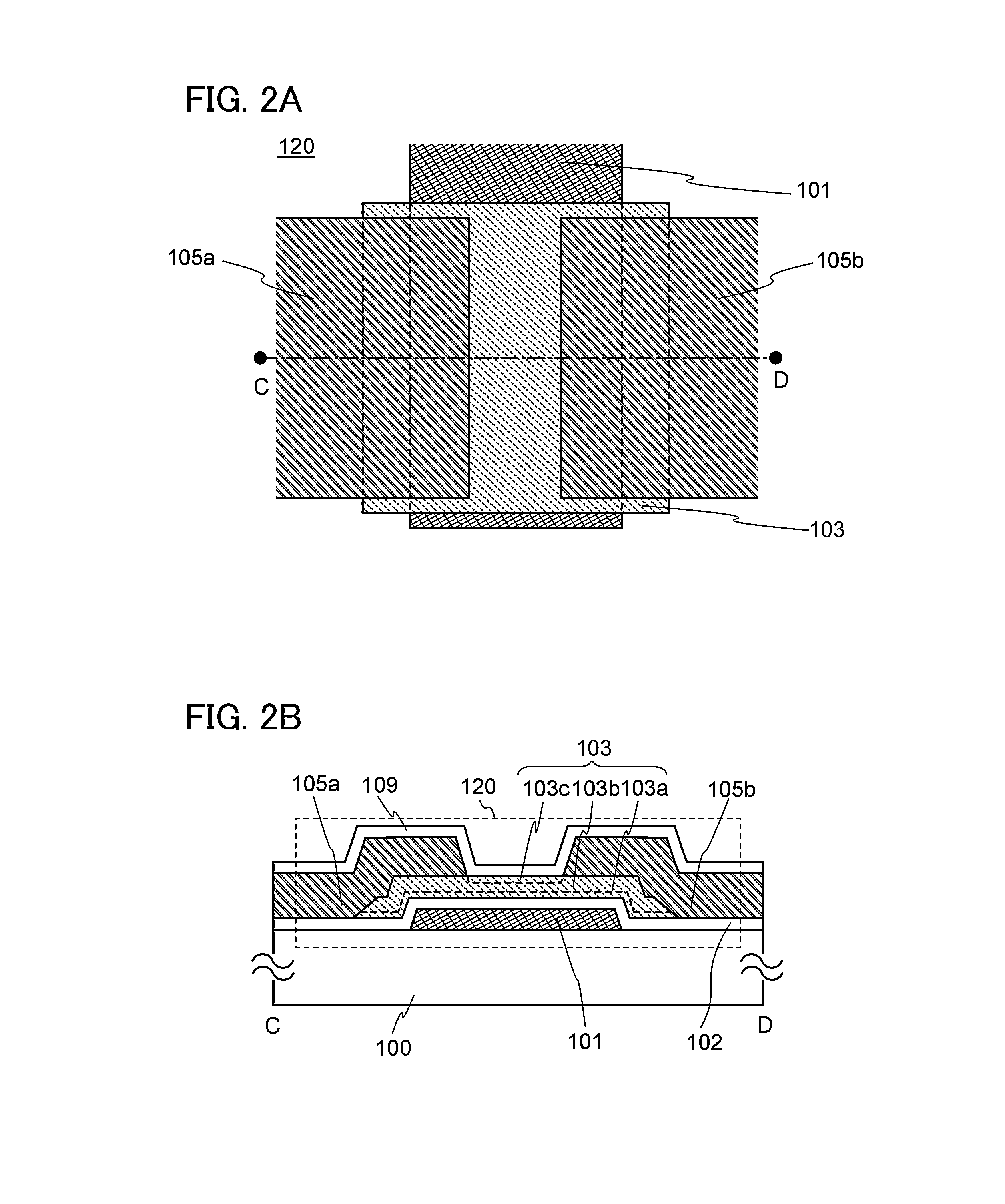
[0056]In FIGS. 1A and 1B, a plan view and a cross-sectional view of a channel-etched type transistor, which has a bottom-gate structure, are shown as an example of a semiconductor device. FIG. 1A is a plan view and FIG. 1B is a cross-sectional view taken along line A-B in FIG. 1A. In FIG. 1A, some of components (e.g., a protective insulating film 109 or the like) of a transistor 110 are omitted to avoid complexity.
[0057]The transistor 110 illustrated in FIGS. 1A and 1B includes, over a substrate 100 having an insulating surface, a gate electrode 101, a gate insulating film 102 covering the gate electrode 101, an oxide semiconductor film 103 provided to be in contact with the gate insulating film 102 and overlap with at least the gate electrode 101, a source elect...
embodiment 2
[0200]A semiconductor device (also referred to as a display device) with a display function can be manufactured using the transistor an example of which is described in Embodiment 1. Moreover, some or all of the driver circuits which include the transistor can be formed over a substrate where the pixel portion is formed, whereby a system-on-panel can be obtained.
[0201]In FIG. 9A, a sealant 4005 is provided so as to surround a pixel portion 4002 provided over a first substrate 4001, and the pixel portion 4002 is sealed by using a second substrate 4006. In FIG. 9A, a signal line driver circuit 4003 and a scan line driver circuit 4004 which are each formed using a single crystal semiconductor film or a polycrystalline semiconductor film over a substrate separately prepared are mounted in a region that is different from the region surrounded by the sealant 4005 over the first substrate 4001. Further, a variety of signals and potentials are supplied to the signal line driver circuit 4003...
embodiment 3
[0259]A semiconductor device disclosed in this specification and the like can be applied to a variety of electronic devices (including game machines). Examples of electronic devices are a television set (also referred to as a television or a television receiver), a monitor of a computer or the like, a camera such as a digital camera or a digital video camera, a digital photo frame, a mobile phone handset (also referred to as a mobile phone or a mobile phone device), a portable game machine, a portable information terminal, an audio reproducing device, a large-sized game machine such as a pachinko machine, and the like. Examples of electronic devices each including the liquid crystal display device described in the above embodiment are described.
[0260]FIG. 13A illustrates a laptop personal computer, which includes a main body 3001, a housing 3002, a display portion 3003, a keyboard 3004, and the like. By applying the semiconductor device described in Embodiment 1 or 2, the laptop per...
PUM
 Abstract
Description
Claims
Application Information