Semiconductor device and method for manufacturing same

Inactive Publication Date: 2013-04-25
SHARP KK
View PDF2 Cites 22 Cited by
  • Summary
  • Abstract
  • Description
  • Claims
  • Application Information

AI Technical Summary

Benefits of technology

[0008]According to the present invention, the performance of the photodiodes formed with the thin film transisto

Problems solved by technology

However, this would greatly increase the number of process steps,

Method used


Image

  • Semiconductor device and method for manufacturing same
  • Semiconductor device and method for manufacturing same
  • Semiconductor device and method for manufacturing same

Examples


embodiment 1

Effects of Embodiment 1

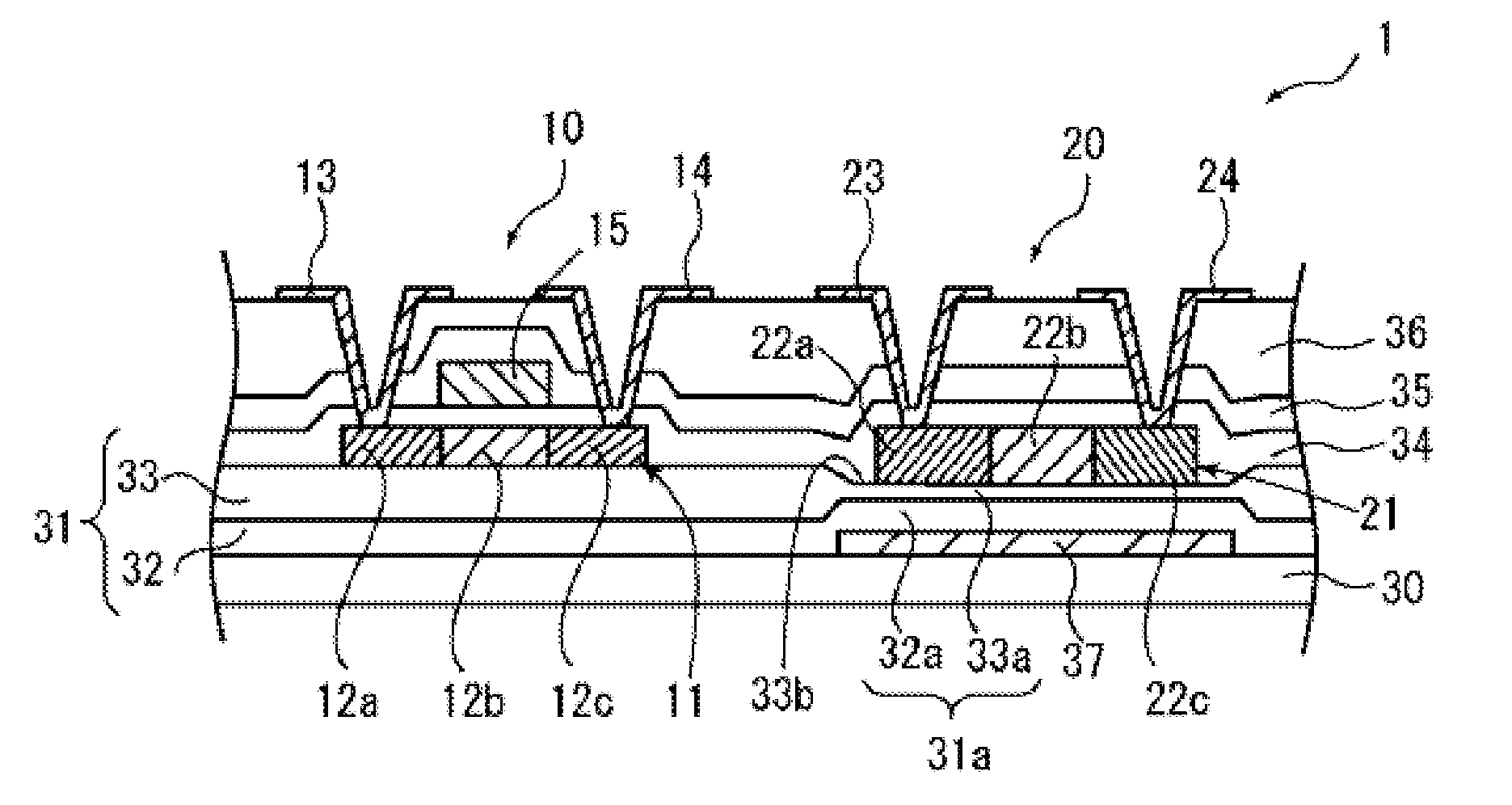
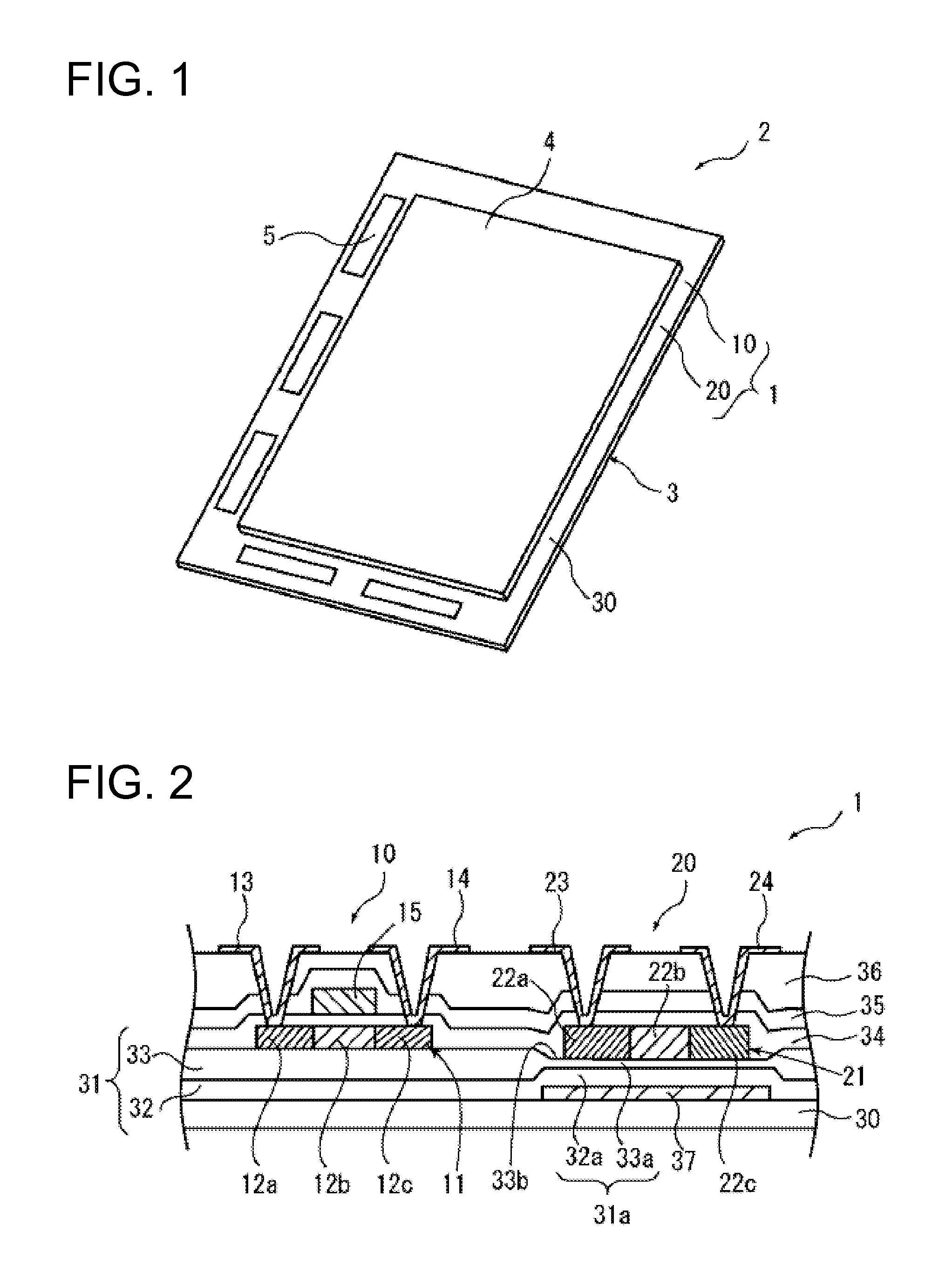
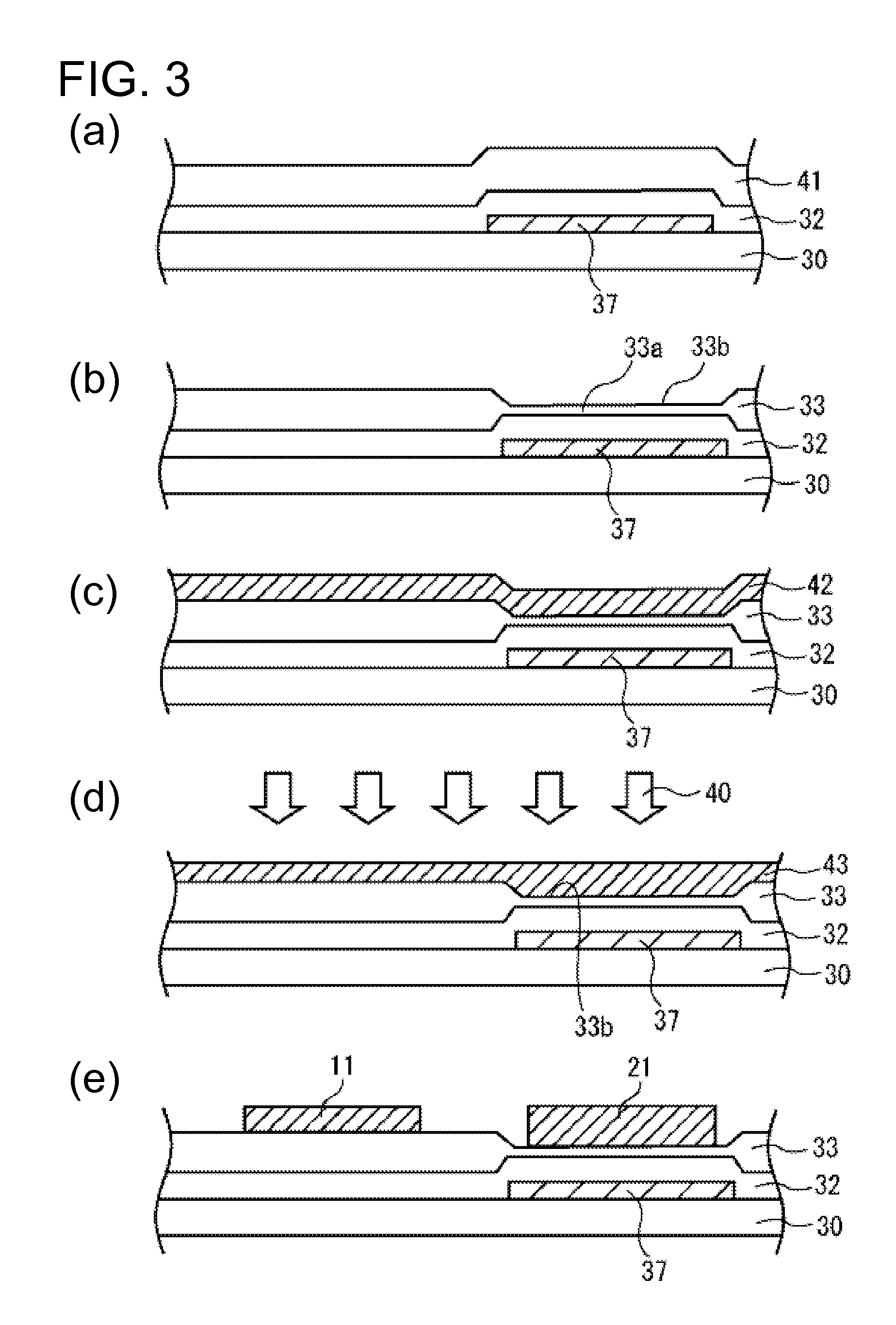
[0064]In the present embodiment, a recess 33b is formed in the silicon oxide film 33a, which serves as a base film for the photodiode 20 in a configuration in which the TFT 10 and the photodiode 20 are provided on the same substrate 30. By melting the silicon thin film 42 formed thereon by radiating a laser beam 40 on the silicon thin film 42, the molten silicon is moved into the recess 33b, making the silicon thin film in the recess 33b thicker than in other parts.

[0065]According to the above configuration, the silicon film 21 of the photodiode 20 can be made thicker than the silicon film 11 of the TFT 10. As a result, the thickness of only the silicon film 21 of the photodiode 20 can be increased without changing the film thickness or characteristics of the TFT, and thus, the sensitivity of the photodiode 20 can be increased.

[0066]Therefore, the manufacturing method of the present embodiment can improve the performance of the photodiode 20 without greatly in...

embodiment 2

Effects of Embodiment 2

[0084]In the present embodiment, the light-shielding film 51 was made to be thinner than the resin film 52, and steps are provided between the light-shielding film 51 and the resin film 52. With this configuration, the silicon film 21 of the photodiode 70 can be made thicker than the silicon film 11 of the TFT 60 without greatly increasing the number of process steps, as in Embodiment 1. Therefore, the performance of the photodiode 70 can be improved.

[0085]Also, the thickness of the silicon nitride film 53 and the silicon oxide film 54 are the same both on the side of the TFT 60 and the side of the photodiode 70. Thus, when a laser beam 40 is radiated onto the silicon thin film 55, the heat distribution on the side of the TFT 60 and the side of the photodiode 70 can be made approximately the same. As a result, the entire silicon thin film 55 can be evenly heated when radiating the laser beam 40 thereon. Therefore, according to the above configuration, the crys...

embodiment 3

Effects of Embodiment 3

[0101]In the present embodiment, the light-shielding film 101 is made thinner than the silicon nitride film 102, and steps are provided between the light-shielding film 101 and the silicon nitride film 102. With this configuration, it is possible to make the silicon film 21 of the photodiode 120 thicker than the silicon film 11 of the TFT 110 without greatly increasing the number of process steps, as in Embodiments 1 and 2. Thus, the performance of the photodiode 120 can be improved.

[0102]In the present embodiment, when etching the silicon nitride film 105, the resist pattern was formed on the silicon nitride film 105 by radiating light from the side opposite to the main surface of the substrate 30, using the light-shielding film 101 as a mask. As a result, it is possible for the region of the silicon nitride film 105 corresponding to the light-shielding film 101 to be etched with ease.

[0103]The thickness of the silicon oxide film 103 is the same both on the s...


PUM


Abstract

Disclosed is a method for manufacturing a semiconductor device that can improve the performance of a photodiode that is formed on a same substrate as a thin film transistor without greatly deteriorating the productivity of the semiconductor device. On a glass substrate 30, a base layer 31 having a recess 33b on the surface is formed, and on the base layer 31, an amorphous silicon thin film 42 is formed. The amorphous silicon thin film 42 is melted to form a crystalline silicon thin film 43, while moving the molten silicon into the recess 33b. Of the silicon thin film 43, a silicon film 11 that constitutes a portion of a thin film transistor 10 is formed of the silicon thin film 43 in a part other than the recess 33b, while a silicon film 21 that constitutes a portion of a photodiode 20 is formed of the silicon thin film 43 in the recess 33b.

Description

TECHNICAL FIELD[0001]The present invention relates to a semiconductor device in which photodiodes and thin film transistors are formed on the same substrate, and a method for manufacturing same.BACKGROUND ART[0002]A semiconductor device in which photodiodes and thin film transistors are formed on the same substrate has been known since before. In such a semiconductor device, the thin film transistors are constituted of some of semiconductor layers out of a plurality of island shaped semiconductor layers formed on the substrate, and the photodiodes are constituted of the remaining semiconductor layers that respectively have light-shielding layers provided between the semiconductor layers and the substrate, as disclosed in Japanese Patent Application Laid-Open Publication No. 2008-300630, for example.SUMMARY OF THE INVENTION[0003]However, when providing photodiodes and thin film transistors on the same substrate as in the configuration disclosed in Japanese Patent Application Laid-Ope...

Claims


Application Information

Patent Timeline
IPC IPC(8): H01L31/113H01L31/18
CPCG02F2001/13312Y02E10/50H01L21/02532H01L21/02658H01L21/02675H01L27/1214H01L29/78633H01L29/78636H01L31/1136H01L31/186H01L27/1218H01L31/02164H01L31/105H01L31/1872H01L21/0243G02F1/13312
Inventor ITOH, TSUYOSHINAKATSUJI, HIROSHIFUJIWARA, MASAHIRO
Owner SHARP KK
Why Eureka
Try Eureka