
Multilayer rare-earth oxide coatings and methods of making

a rare earth oxide and coating technology, applied in the field of rare earth oxide coatings and multi-layer rare earth oxide coatings and making methods, can solve the problems of oxidation and/or erosion of these surfaces, weakening the underlying structure, and complication that can occur, and achieve the effect of controlling the roughness/smoothness of the coating

Inactive Publication Date: 2013-05-09
COORSTEK INC
View PDF8 Cites 31 Cited by
  • Summary
  • Abstract
  • Description
  • Claims
  • Application Information

AI Technical Summary

Benefits of technology

The patent describes a way to protect processing equipment (like semiconductor fabrication chambers) from corrosion, abrasion, and oxidation damage. This is done by applying a coating made of rare-earth oxide, rare-earth fluoride, rare-earth silicate, or rare-earth oxyfluoride to the exposed surfaces of the equipment. The coating is rough enough to allow for a second layer (a dielectric layer) to be securely attached to it but smooth enough to prevent pieces of the coating from breaking off during processing. After exposure to processing materials, the second layer is removed and replaced with a new layer to continue the protection of the equipment. This method helps to keep the equipment clean and precise during processing.

Problems solved by technology

This exposure may lead to oxidation and / or erosion of these surfaces.
This oxidation or erosion may weaken the underlying structures.
A second complication that can occur is the redeposition of the material of the chamber surface onto the substrate being processed.
This can lead to imperfections: the redeposition of chamber surface material may weaken the bond between a layer and the substrate, or it can provide unwanted masking in an etch process.
A third problem results from chemical effects.
In turn, this may produce undesirable changes in etch rate or deposition.

Method used


Image

  • Multilayer rare-earth oxide coatings and methods of making
  • Multilayer rare-earth oxide coatings and methods of making
  • Multilayer rare-earth oxide coatings and methods of making

Examples


example 2

[0044] A large ceramic disk was coated with yttria using thermal plasma spray. The coating was about 100 μm thick and contained about 3% porosity.

[0045]A CO2 laser beam was scanned across the disk using the following conditions:

EquipmentEpilog Legend 36XTPower  75 WScan speed  80 cm / sSpot size~100 umGas flow  20 slmGas composition10% CH4, bal. Ar

[0046]The gas was injected coaxially with the beam. After this process, the initially white coating turned black. Inspection in an electron microscope of fractured sections showed melting of the top surface to a depth of about 10 μm. The same area was then treated with a Q-switched Nd:YAG laser in open air using the following conditions:

EquipmentLumonics LightWriterSPePower  40 WScan speed  15 cm / sSpot size~100 umPulse rate 1.5 kHz

[0047]The coating remained black. Inspection of a cross-section in an optical microscope indicated that the black color penetrated at least 5 μm down from the surface. FIGS. 3E and 3F show respectively the top surf...

example 3

[0048] A set of 25 mm diameter ceramic disks was coated with yttria using thermal plasma spray in a manner similar to Example 2. Again, the coating was about 100 μm thick and contained about 3% porosity. A CO2 laser beam was scanned across the disk using the following conditions, which are similar to Example 2:

EquipmentEpilog Legend 36XTPower  75 WScan speedVariableSpot size~100 umGas flow  20 slmGas composition10% CH4, bal. Ar

[0049]Half of the coupons were scanned at 60 cm / s and half at 80 cm / s. Four of the coupons were subjected to the following crack measurement procedure. At least 3 randomly chosen locations on each coupon were imaged in the SEM at 1000× (field 1280×960 pixels, scale 1 pixel=0.104 μm).

[0050]Each field was reviewed for cracks. The maximum crack width per field was measured from the image using the following criteria:[0051]measurements were done away from chips, pores and lumps in the coating[0052]the width needed to be reasonably constant for 3 or more crack widt...


PUM

PropertyMeasurementUnit
Lengthaaaaaaaaaa
Lengthaaaaaaaaaa
Lengthaaaaaaaaaa

Abstract

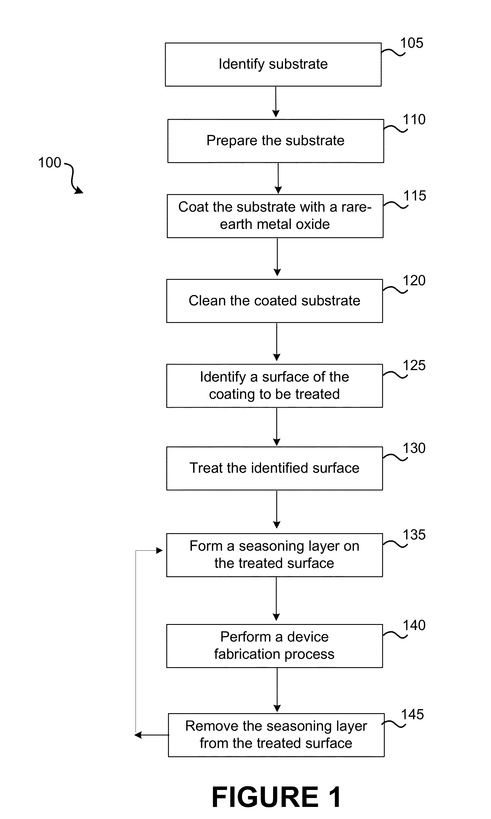
Embodiments relate to a coated substrate and a method of making and using the same. A plasma-spray coated layer may be formed on a substrate, wherein the plasma-sprayed coated layer comprises a rare-earth oxide (e.g., yttrium oxide), a rare-earth fluoride (e.g. yttrium fluoride), or a rare-earth silicate (e.g. yttrium silicate). An exposed surface of the plasma-spray coated layer may be irradiated to form a treated portion of the layer, wherein the treated portion of the layer has a mean spacing of local peaks (S value) between about 100 and 200 microns. A second layer may be formed on the treated portion of the plasma-spray coated layer, wherein the second layer comprises a dielectric material.

Description

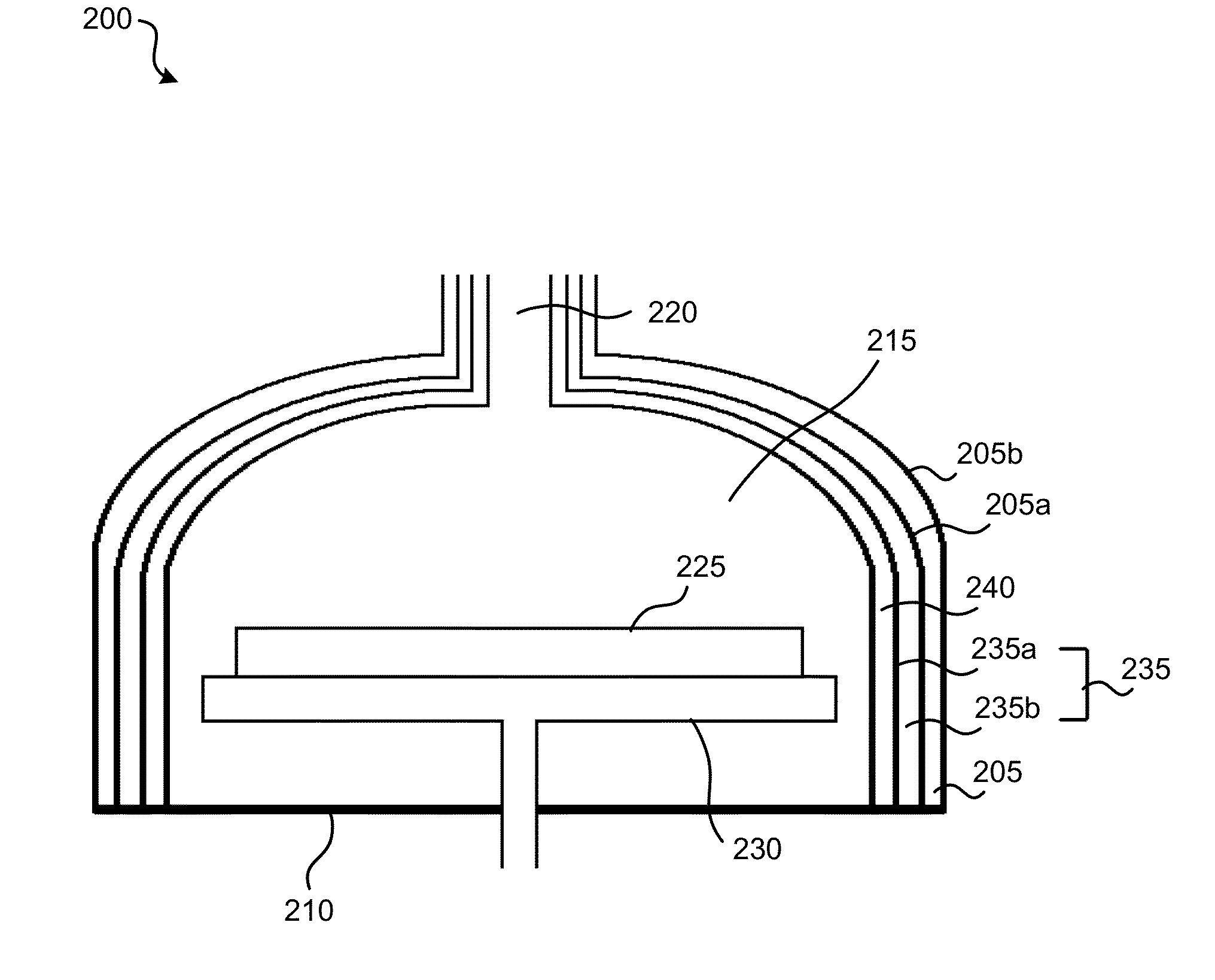
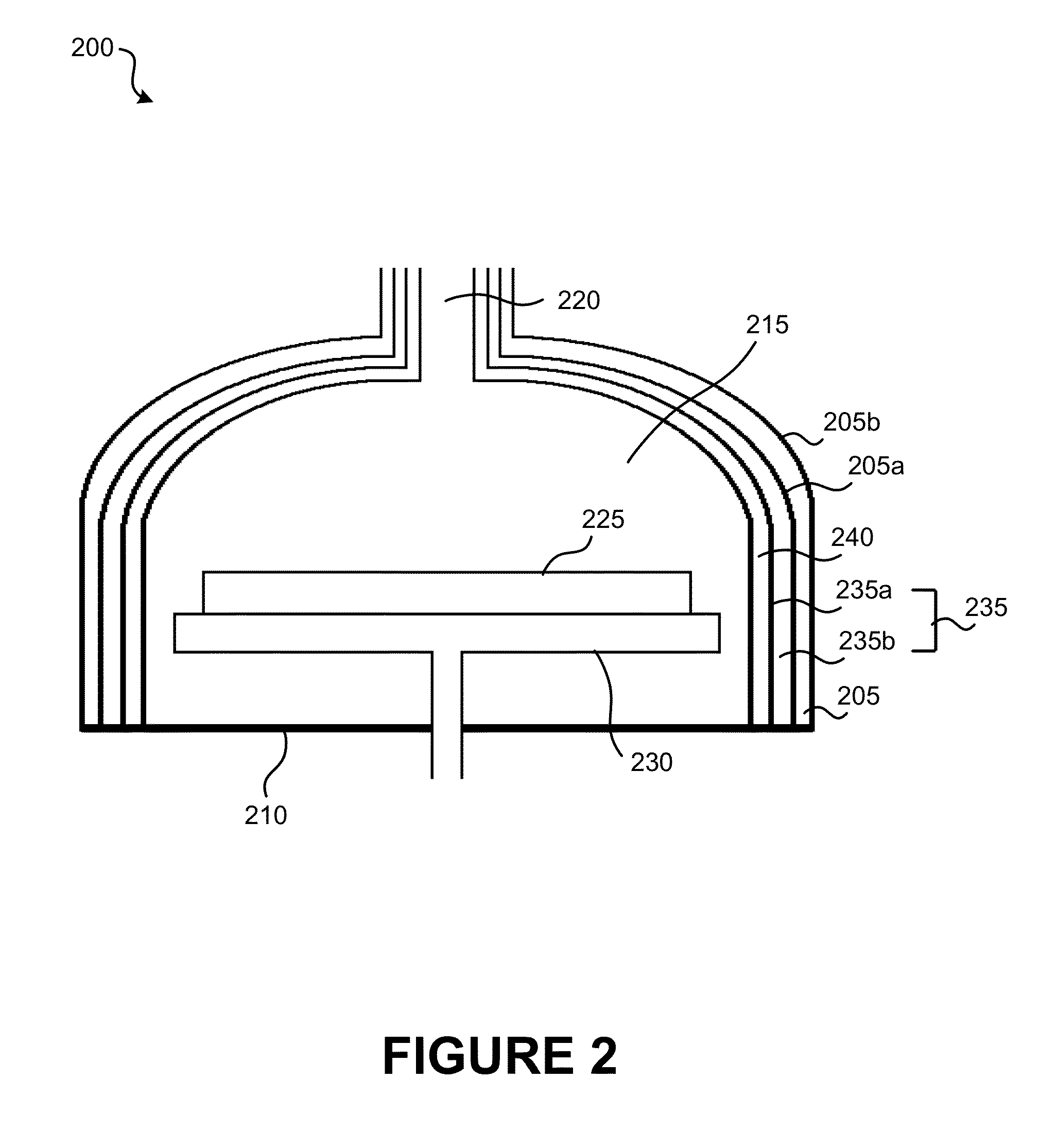
CROSS-REFERENCE TO RELATED APPLICATIONS[0001]This application is a non-provisional of and claims the benefit and priority of U.S. Application No. 61 / 555,274, filed on Nov. 3, 2011, which is hereby incorporated by reference in its entirety for all purposes.BACKGROUND OF THE INVENTION[0002]Semiconductor devices are frequently fabricated in a chamber. Layers may be deposited onto a substrate by, e.g., sputtering a compound onto the substrate. The layers may be shaped into specific geometries by etching the layers, which may involve introducing a corrosive gas into the chamber. Thus, surfaces inside the chamber (e.g., inner surfaces of a chamber's housing) may be exposed to sputtered compounds and etchants. This exposure may lead to oxidation and / or erosion of these surfaces. This oxidation or erosion may weaken the underlying structures. A second complication that can occur is the redeposition of the material of the chamber surface onto the substrate being processed. This can lead to i...

Claims


Application Information

Patent Timeline
IPC IPC(8): C23C4/12B32B9/04B32B33/00
CPCC23C4/02C23C4/10Y10T428/24355C23C4/18C23C4/105C23C4/11
Inventor YOUNG-DOHE, ELIZABETHANDERSON, FRANK E.SIMPSON, MATTHEW
Owner COORSTEK INC
Learn More