

Organic electroluminescence element
- Summary
- Abstract
- Description
- Claims
- Application Information
AI Technical Summary
Benefits of technology
Problems solved by technology
Method used
Image

Examples
embodiment 1
Structure of Organic EL Element
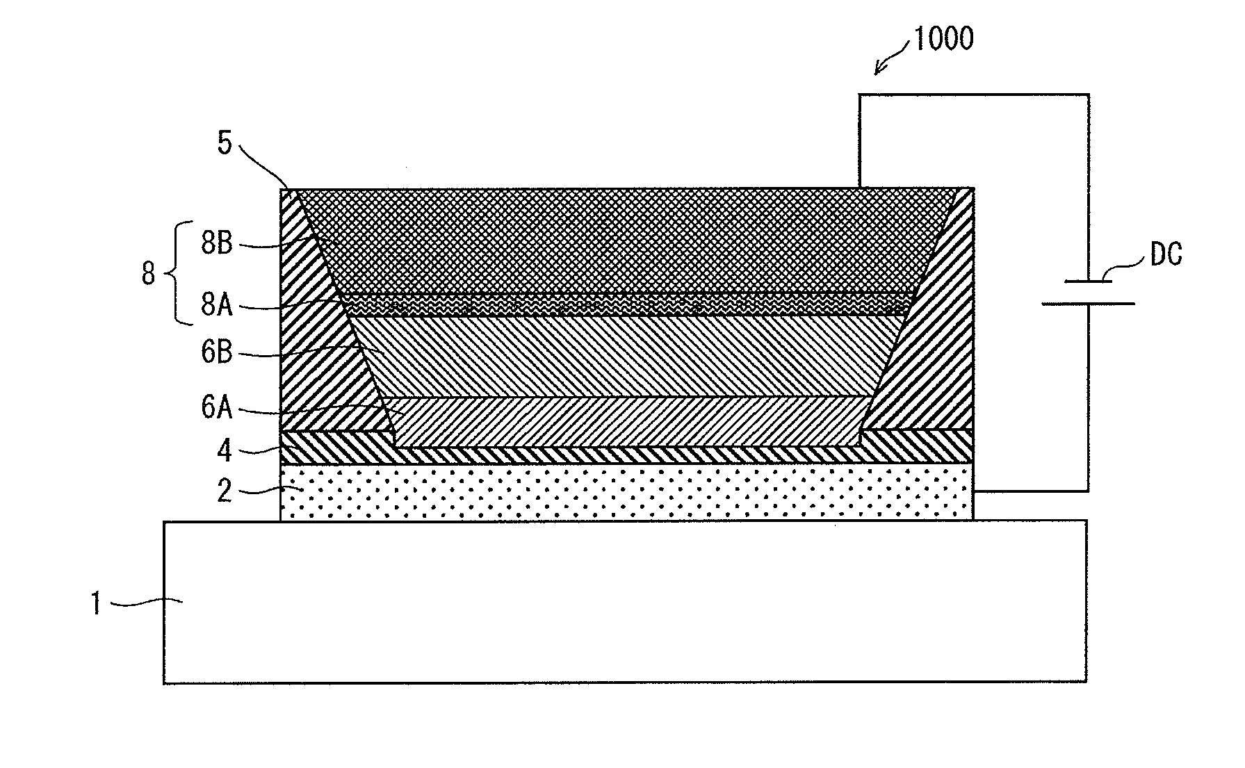
[0074]FIG. 1 is a schematic cross-sectional view illustrating the structure of an organic EL element 1000 pertaining to the present embodiment.
[0075]The organic EL element 1000 is an application-type organic EL element, which is characterized in that a functional layer is applied by a wet process in the manufacturing thereof. The organic EL element 1000 includes: a hole injection layer 4; a functional layer including various layers (a buffer layer 6A and a light-emitting layer 6B, in this case); and a pair of electrodes composed of an anode 2 and a cathode 8. The hole injection layer 4 and the functional layer are disposed one on top of the other, and are disposed between the pair of electrodes. Each layer of the functional layer contains organic material having a predetermined function.
[0076]More specifically, the organic EL element 1000 includes, as illustrated in FIG. 1, the anode 2, the hole injection layer 4, the buffer layer 6A, the light-emittin...
embodiment 2
Overall Structure of Light-Emitting Element
[0217]FIG. 16 is a schematic view illustrating a layered state of layers of a light-emitting element 1000C pertaining to embodiment 2. FIG. 17 is an enlarged view of a part surrounded by dashed-dotted lines in FIG. 16.
[0218]As illustrated in FIG. 16, the light-emitting element 1000C is a top emission type organic light-emitting element in which pixels corresponding to the colors R, G, and B are arranged so as to form lines or to form a matrix. Further, each pixel has a layered structure where various layers are layered above the substrate 1.
[0219]The light-emitting element 1000C differs from the organic EL element 1000 in embodiment 1 in that, in the light-emitting element 1000C, the hole injection layer 4 is disposed on an upper surface of an anode (the anode 2) with an ITO layer 3 interposed therebetween. In addition, the light-emitting element 1000C also differs from the organic EL element 1000 in embodiment 1 in that (i) the buffer laye...
embodiment 3
[0260]A light-emitting element 1000D pertaining to embodiment 3 differs greatly from the light-emitting element 1000C pertaining to embodiment 2 in that the ITO layer is not formed under the hole injection layer and that a protection film is formed on the hole injection layer. In the following, description is provided while focusing on aspects differing from embodiment 2 and while simplifying or omitting description concerning aspects that are similar to embodiment 2.
[0261](Structure of Light-emitting Element 1000D)
[0262]FIG. 24 is a schematic view illustrating a layered state of layers of the light-emitting element 1000D. As illustrated in FIG. 24, the light-emitting element 1000D includes an anode 102 formed on a substrate 101, and a hole injection layer 104 and a protective layer 110 that are layered on the anode 102 in the stated order. The hole injection layer 104 functions as a charge injection transport layer. Here, note that the hole injection layer 104 is formed across the ...
PUM
 Abstract
Description
Claims
Application Information