Electron multiplier detector formed from a highly doped nanodiamond layer

a nanodiamond layer and detector technology, applied in the field of electromagnetic radiation or ion flow detection systems comprising electron multipliers in transmission, can solve the problems of low mechanical strength of diamond layers of such thicknesses, high cost of image intensifier tubes, and particularly long and complex tubes

Active Publication Date: 2013-06-13
PHOTONIS FRANCE
View PDF0 Cites 14 Cited by
  • Summary
  • Abstract
  • Description
  • Claims
  • Application Information

AI Technical Summary

Benefits of technology

[0036]In fact, the nanocrystalline structure of the B-NCD diamond layer as well as the high concentration of boron atoms make the diffusion of secondary electrons particularly important and reduce their mobility.
[0061]Finally, it should be noted that the casing of the detection system comprises fewer parts to assemble than that of the prior art cited previously. The risks of a sealing defect between the parts forming the casing are then reduced. In addition, the casing is shorter and lighter, which meets the normal constraints of use of detection systems such as image intensifier tubes, photomultiplier tubes and ion flow detection tubes.

Problems solved by technology

In addition, the method for manufacturing the tube is rendered particularly long and complex, which leads to a high cost of the image intensifier tube.
However, a diamond layer of such a thickness has low mechanical strength, which necessitates using means for maintaining and reinforcing the diamond layer.

Method used


Image

  • Electron multiplier detector formed from a highly doped nanodiamond layer
  • Electron multiplier detector formed from a highly doped nanodiamond layer
  • Electron multiplier detector formed from a highly doped nanodiamond layer

Examples


first embodiment

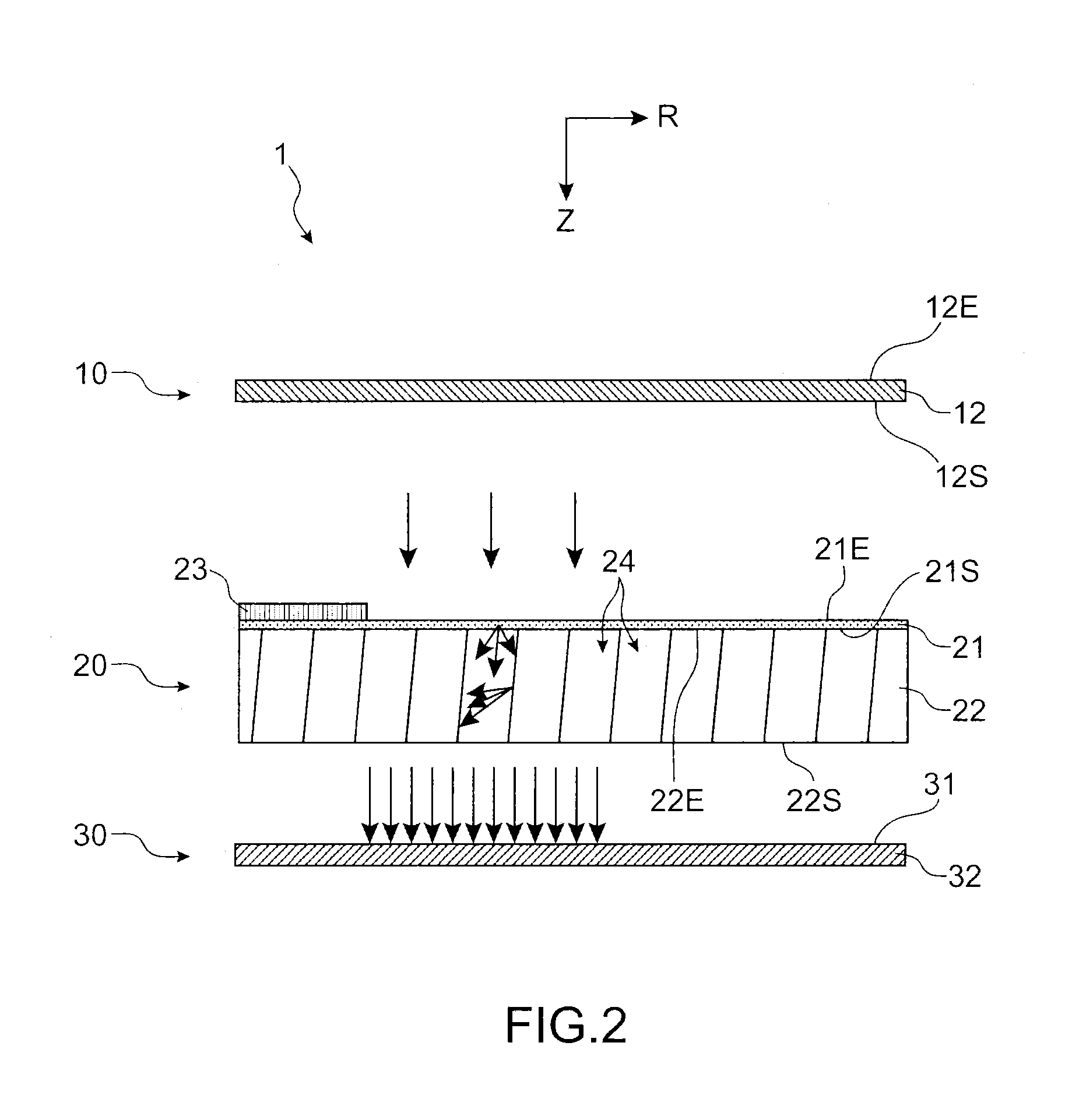
[0075]FIG. 2 illustrates partially and in a schematic manner an image intensifier tube according to the invention.

[0076]It should be noted that the scales are not respected in order to favour the clarity of the drawing.

[0077]Throughout the description that follows, an orthonormal mark (R,Z) in cylindrical coordinates is used where R is the radial direction of the tube and Z is the axial direction of the tube, which may also be substantially assimilated with the general direction of propagation of the electrons.

[0078]Furthermore, the terms “upstream” and “downstream” used hereafter should be understood herein in terms of orientation along the direction Z of the mark (R,Z).

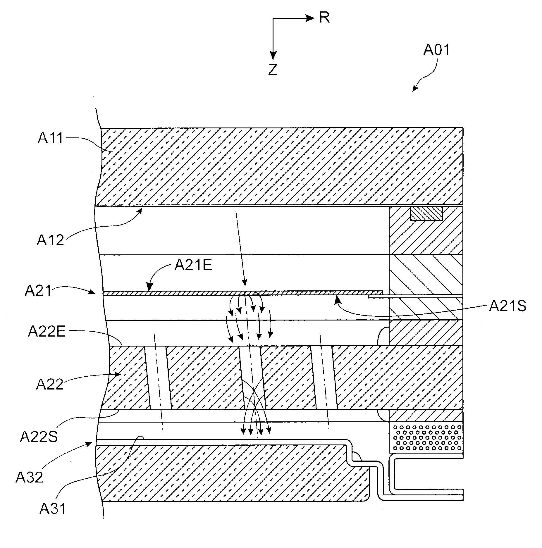
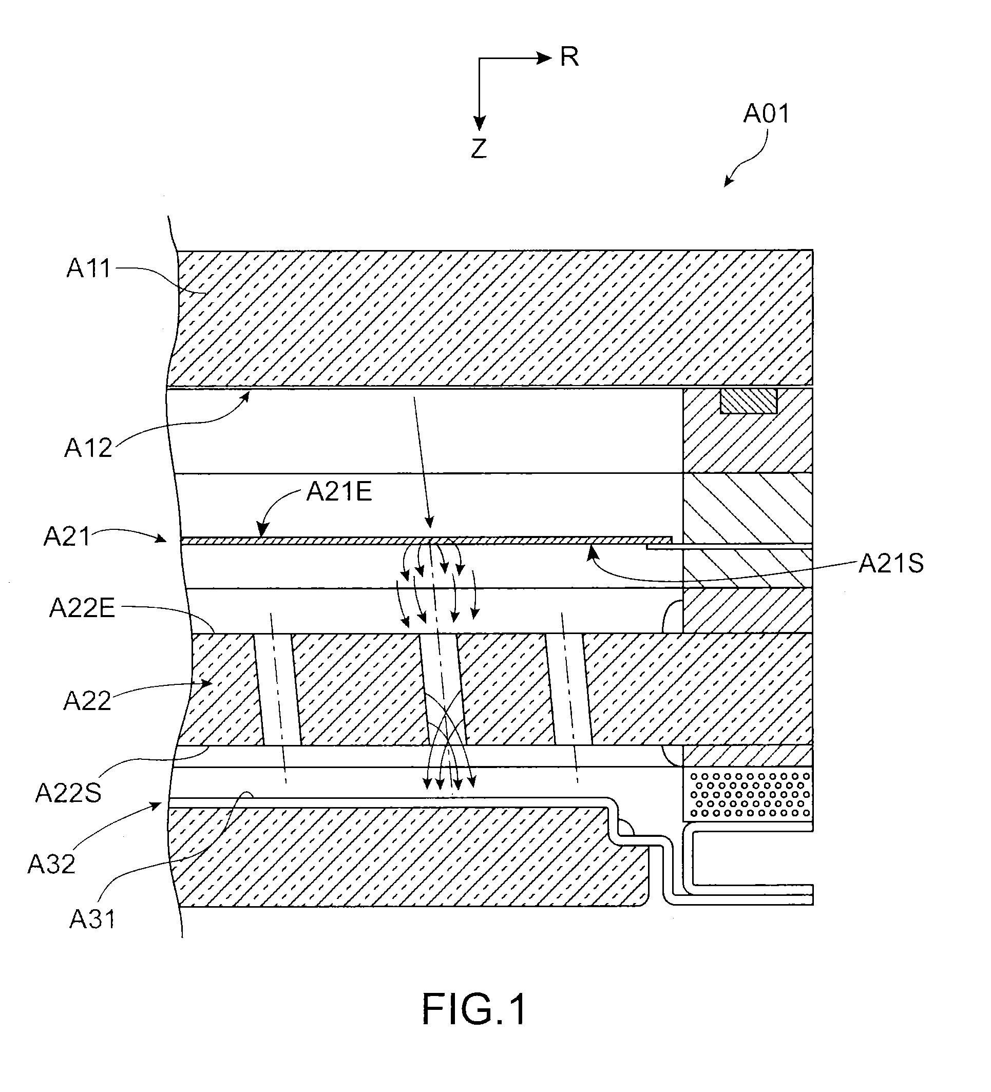
[0079]In FIG. 2 is represented an image intensifier tube 1 according to the first embodiment of the invention. The tube 1 has a substantially cylindrical or tubular shape along the Z axis. However, the tube 1 may also have a square, rectangular, hexagonal section shape, or any other shape.

[0080]The tube 1 comprises ...

second embodiment

[0145]FIG. 4 is a partial schematic view of an image intensifier tube according to the invention.

[0146]Identical numerical references to those of FIG. 2 described previously designate identical or similar elements.

[0147]The image intensifier tube according to this embodiment differs essentially from the first embodiment described with reference to FIG. 2 in that the B-NCD diamond layer 21 is arranged between the MCP 22 and the output device 30, and in contact therewith.

[0148]It is thus not necessary to generate an electric field between the B-NCD diamond layer 21 and the output device 30.

[0149]The operation of the image intensifier tube according to this embodiment is similar to that of the tube described previously and is not described again here.

[0150]FIG. 5 is a partial schematic view of an image intensifier tube according to a variant of the second embodiment of the invention.

[0151]Identical numerical references to those of FIG. 4 described previously designate identical or simi...

third embodiment

[0160]FIG. 6 is a partial and schematic view of an image intensifier tube according to a

[0161]Identical numerical references to those of FIG. 2 described previously designate identical or similar elements.

[0162]The image intensifier tube according to this variant differs from the first embodiment described previously in that the electron multiplier no longer comprises a MCP but, quite the opposite, a plurality of B-NCD diamond layers 21 arranged one on another along the Z axis of the tube and spaced apart from each other.

[0163]The diamond layers may be arranged at a distance from each other comprised between several microns and several hundreds of microns, for example between 5 μm and 500 μm, and preferably between 30 μm and 500 μm, for example 50 μm.

[0164]As shown in FIG. 6, the collection electrode 23 may be arranged at the edge of the upstream face 21E of the diamond layer.

[0165]Alternatively, the collection electrode 23 of the upstream face 21E of each B-NCD diamond layer 21 may...


PUM


Abstract

A system for detecting electromagnetic radiation or an ion flow, including an input device for receiving the electronic radiation or the ion flow and emitting primary electrons in response, a multiplier of electrons in transmission, for receiving the primary electrons and emitting secondary electrons in response, and an output device for receiving the secondary electrons and emitting an output signal in response. The electron multiplier includes at least one nanocrystalline diamond layer doped with boron in a concentration of higher than 5·1019 cm−3.

Description

TECHNICAL FIELD[0001]The present invention relates to the general field of systems for detecting electromagnetic radiation or ion flow comprising a multiplier of electrons in transmission. By way of example, photomultiplier tubes, image intensifier tubes, or instead, ion detection tubes may be cited.[0002]Multiplier of electrons in transmission is taken to mean a device capable of receiving incident electrons and emitting so-called secondary electrons in response in high numbers. The incident electrons impact the device on a receiving face and the secondary electrons are emitted from an opposite emitting face.PRIOR ART[0003]Conventionally, a system for detecting electromagnetic radiation or ion flow comprises an input device for receiving an electromagnetic radiation or an ion flow and emitting in response a flux of so-called primary electrons, a multiplier of electrons potentially in transmission for receiving the primary electrons and emitting so-called secondary electrons in resp...

Claims


Application Information

Patent Timeline
Patent Type & Authority Applications(United States)
IPC IPC(8): G01T1/24H01J43/04
CPCH01J1/32H01J29/023H01J31/48H01J31/49H01J31/506H01J43/04H01J43/246H01J2231/5001H01J2231/50047B82Y15/00G01T1/247H01J43/22
Inventor NUETZEL, GERTLAVOUTE, PASCALJACKMAN, RICHARD B.
Owner PHOTONIS FRANCE
Why Eureka
Try Eureka