
Alloy wire and methods for manufacturing the same

a technology of alloy wires and manufacturing methods, applied in the direction of metallic material coating process, surface reaction electrolytic coating, solid-state devices, etc., can solve the problems of generating electron migration, local coarse grains formed, negatively affecting bonding strength

Inactive Publication Date: 2013-07-04
WIRE TECH CO LTD
View PDF10 Cites 26 Cited by
  • Summary
  • Abstract
  • Description
  • Claims
  • Application Information

AI Technical Summary

Benefits of technology

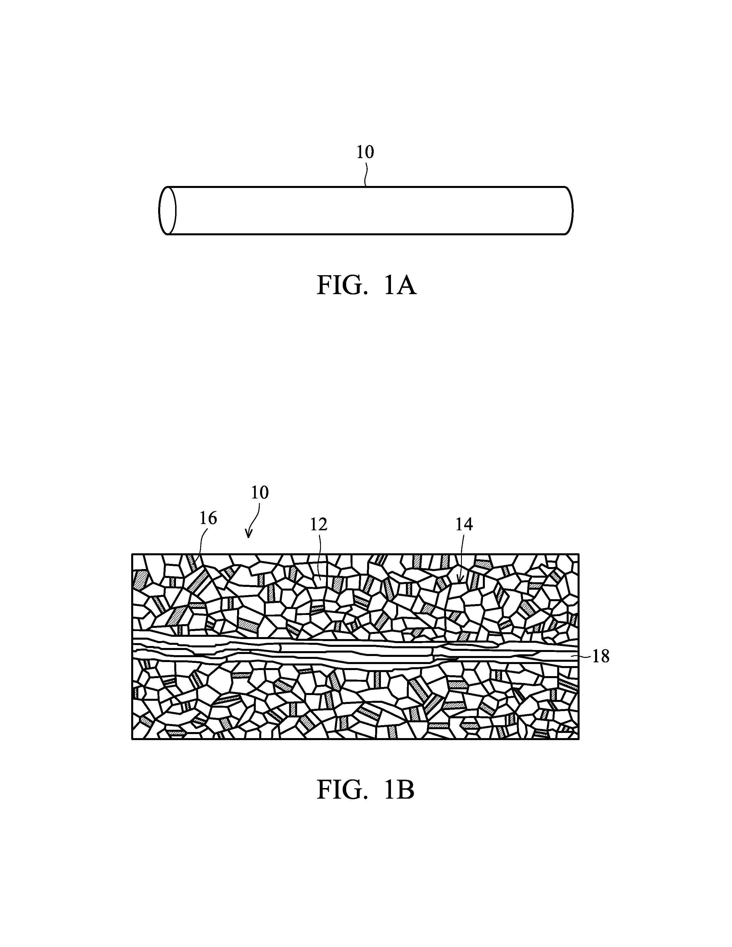
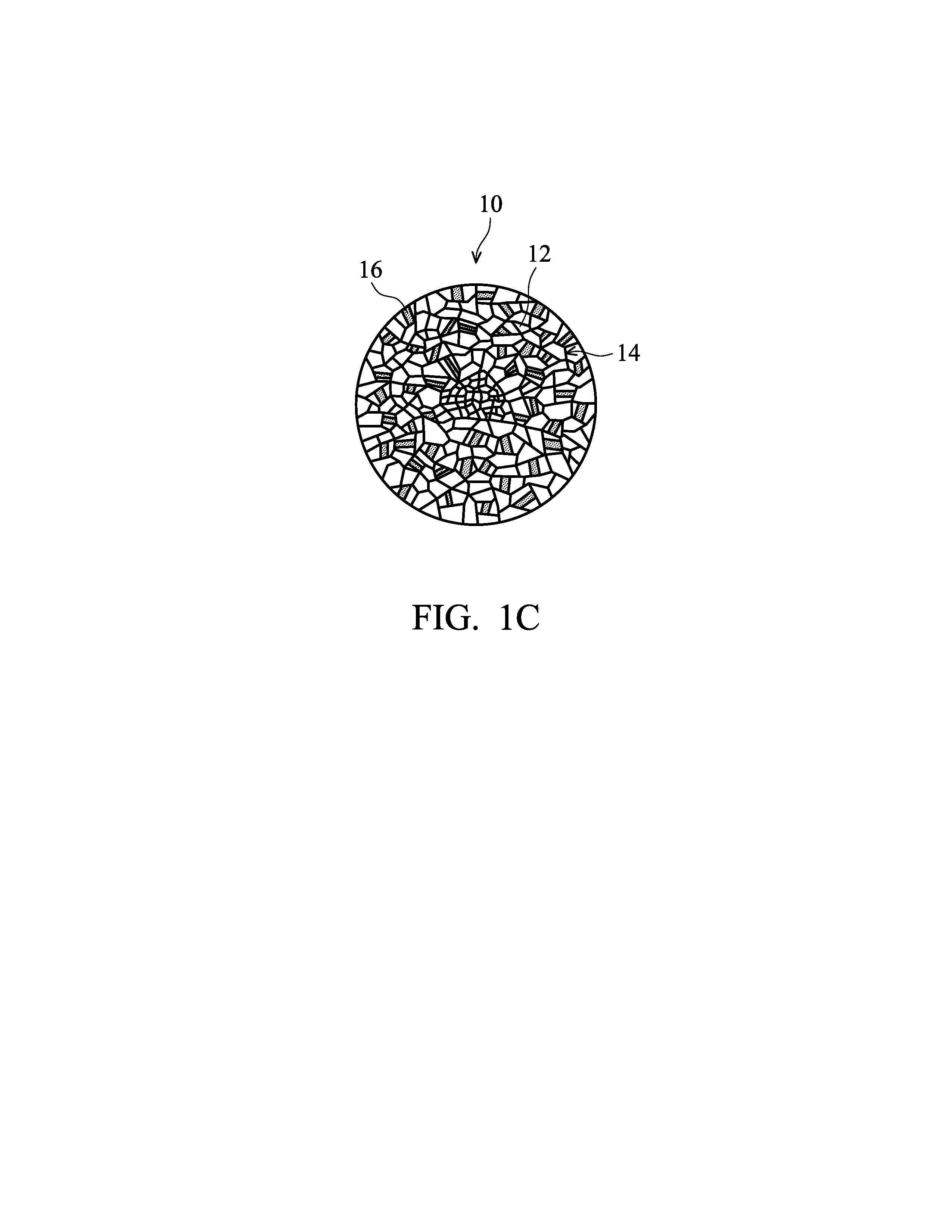
The invention provides an alloy wire made of a material selected from the group consisting of a silver-gold alloy, a silver-palladium alloy, and a silver-gold-palladium alloy. The alloy wire has a polycrystalline structure of a face-centered phase and comprises a plurality of grains. The grains include slender grains or equi-axial grains. The alloy wire has a wire diameter between 10 μm and 50 μm. The alloy wire can be made by a method involving steps of melting raw materials, casting, cold work shaping, and plating a metal coating. The technical effects of the invention include improved mechanical properties, such as high strength and ductility, as well as improved electrical properties, such as high conductivity and low resistivity.

Problems solved by technology

Grain growth happens to the metal wire in the heat affected zone due to heat build-up, resulting in formation of local coarse grains.
The local coarse grains provide a lower strength, and thus, the metal wire cracks in the heat affected zone during the wire pull test, negatively affecting the bonding strength.
When completing the packaging processes of the semiconductor devices or the light emitting diodes, the high current density through the metal wires potentially activate atoms in the metal wires and thus generate electron migration during utilization of the packaged products.
As a result, holes are formed at the terminal of the metal wires, resulting in a decrease in electrical conductivity and thermal conductivity, and even the occurrence of broken wires.
However, there are a lot of high angle grain boundaries existing between the fine grains.
The high angle grain boundaries scatter the electron transmission, and thus increase the electrical resistivity of the metal wires and simultaneously decrease the thermal conductivity of the metal wires.
On the other hand, the high angle grain boundaries have higher interfacial energy and provide favorable paths for environmental oxidation, sulfuration and chloride ion corrosion, lowering the reliability of packaged electronic products.
Thus, the wire bonding strength is decreased, and electron migration tends to occur to the metal wire with a fine grain structure during utilization of packaged semiconductor devices or light emitting diodes, which are all main factors causing the deterioration of quality and reliability of conventional packaged products utilizing wire bonding technology.

Method used


Image

  • Alloy wire and methods for manufacturing the same
  • Alloy wire and methods for manufacturing the same
  • Alloy wire and methods for manufacturing the same

Examples


example 1

[0070]A siver-8 wt % gold-3 wt % palladium alloy is smelted by high frequency electric smelting, followed by continuous casting to form a thick wire with a wire diameter of 6 mm. The thick wire becomes a fine wire with a wire diameter of 22.6 μm after a plurality of steps of wire drawing elongation and annealing treatment, followed by performance of the second-last step of wire drawing elongation, becoming a fine wire with a wire diameter of 20 μm. Next, the fine wire is annealed at 530° C. for 1.5 seconds, followed by performance of the last step of wire drawing elongation, becoming a fine wire with a wire diameter of 17.5 μm. Finally, the last step of the annealing treatment is performed on the fine wire at an annealing temperature of 570° C. for 4.8 seconds. Completing the last step of the annealing treatment, the fine wire is wound, and then an alloy wire product for wire bonding is complete.

[0071]In order to verify that plenty of annealing twin structures contribute to the exce...

example 2

[0093]A siver-8 wt % gold-3 wt % palladium alloy is smelted by high frequency electric smelting, followed by continuous casting to form a thick wire with a wire diameter of 6 mm. The thick wire becomes a fine wire with a wire diameter of 22.6 μm after a plurality of steps of wire drawing elongation and annealing treatment, followed by performance of the second-last step of wire drawing elongation, becoming a fine wire with a wire diameter of 20 μm. Next, the fine wire is annealed at 650° C. for 10 seconds, followed by performance of the last step of wire drawing elongation, becoming a fine wire with a wire diameter of 17.5 μm. Finally, the last step of the annealing treatment is performed on the fine wire at an annealing temperature of 700° C. for 60 seconds. Completing the last step of the annealing treatment, the fine wire is wound, and then an alloy wire product for wire bonding is complete.

[0094]A photograph of a Metallography structure along a lengthwise cross-section of the in...


PUM

PropertyMeasurementUnit
weight percentaaaaaaaaaa
diameteraaaaaaaaaa

Abstract

An alloy wire made of a material selected from one of a group consisting of a silver-gold alloy, a silver-palladium alloy and a silver-gold-palladium alloy is provided. The alloy wire is with a polycrystalline structure of a face-centered cubic lattice and includes a plurality of grains. A central part of the alloy wire includes slender grains or equi-axial grains, and the other parts of the alloy wire consist of equi-axial grains. A quantity of the grains having annealing twins was 20 percent or more of the total quantity of the grains of the alloy wire.

Description

CROSS REFERENCE TO RELATED APPILCATIONS[0001]This Application claims priority of Taiwan Patent Application No. 101100014, filed on Jan. 2, 2012, the entirety of which is incorporated by reference herein.BACKGROUND OF THE INVENTION[0002]1. Field of the Invention[0003]The invention relates to alloy wires and manufacturing methods thereof, and more specifically to alloy wires utilized for wire bonding of packages of electronic devices and manufacturing methods thereof.[0004]2. Description of the Related Art[0005]Wire bonding is an extremely important step in the packaging processes of semiconductor devices and light emitting diodes (LED). Bonding wires provide not only signal transmission and power transmission between chips and chip carriers (substrates), but also heat dissipation performance. Therefore, it is necessary for metal wires for wire bonding to have not only excellent electrical conductivity and thermal conductivity, but also sufficient strength and ductility. The hardness ...

Claims


Application Information

Patent Timeline
Patent Type & Authority Applications(United States)
IPC IPC(8): B32B15/01C22C5/06C22F1/14B32B15/02
CPCH01L2224/43B32B15/018C22F1/14H01L23/48H01L24/45H01L2224/45139H01L2224/45565H01L24/43H01L2224/45015H01L2224/45644H01L2224/45664C22C5/06Y10T428/12875Y10T428/12889Y10T428/12868H01L2224/43848H01L2924/12041H01L2924/00014H01L2924/01006H01L2924/01047H01L2924/01015H01L2224/45147H01L2224/45144H01L2224/45124H01L2924/01079H01L2924/01046H01L2924/2075H01L2924/20751H01L2924/20752H01L2924/20753H01L2924/20754H01L2924/20755H01L2924/0132H01L2924/00015H01L2924/013H01L2924/00H01L2924/00011H01L2224/45669H01L2224/45647H01L2924/01204H01L2224/48H01L2224/43986Y10T428/12431Y10T428/12438Y10T428/12896H01L2924/00013H01L2224/4321H01L2924/01049H01L2924/01045H01L2924/01004H01L2924/01005B22D25/02C23C30/00
Inventor LEE, JUN-DERTSAI, HSING-HUACHUANG, TUNG-HAN
Owner WIRE TECH CO LTD
Learn More