Biopolymer Optical Analysis Device and Method

a biopolymer and optical analysis technology, applied in the direction of optical radiation measurement, instruments, spectrometry/spectrophotometry/monochromators, etc., can solve the problems of mechanical instability, reduce the effective cross-sectional area, reduce the ionic current, etc., to achieve high constructive stability and reliability, and improve the ability to identify bases. , the effect of high ability to identify bases

Active Publication Date: 2013-07-11
HITACHI HIGH-TECH CORP
View PDF7 Cites 39 Cited by
  • Summary
  • Abstract
  • Description
  • Claims
  • Application Information

AI Technical Summary

Benefits of technology

[0023]The present invention provides a biopolymer property analysis chip. The property analysis chip of the present invention using a solid state nanopore method has advantageous in that it has high constructive stability and reliability compared with a bionanopore-based chip using a bilayer membrane method.
[0024]The analysis chip of the present invention analyses a biopolymer using the Raman scattering spectrum as an indicator to determine the types of the monomers contained in the biopolymer. The spectrum having two-dimensional information, namely a wavenumber or wavelength-intensity pattern, contains an exponentially large volume of information and has a high ability of identify bases in qualitative analysis, compared with one-dimensional information, for example, tunneling current intensity. Accordingly, the present invention has an extremely higher ability to identify bases than that of the nanopore by means of tunneling current.
[0025]Moreover, the property analysis chip with multinanopore of the present invention is capable of analyzing a plurality of biopolymers concurrently in parallel using a spectrooptics, which measures a plurality of spectra in parallel. For this reason, the property analysis chip with multinanopore of the present invention achieved high throughput compared with analysis devices and methods according to prior art.
[0026]Furthermore, the present invention provides a biopolymer property analysis device and method. The property analysis device of the present invention is capable of controlling the speed at which the biopolymer penetrates into the nanopore, and eliminating the need for a step of immobilizing the biopolymer to be analyzed on the solid state substrate in advance and the need for a complicated device, for example, a high-resolution high precision stage or Atomic Force Microscope (AFM). In addition, the need for a delicate step of causing the AFM probe to scan two-dimensionally at the accuracy of sub-nm, is eliminated. For this reason, the device construction and operation of the property analysis device of the present invention is simpler than those in analysis using the TERS method according to prior art.

Problems solved by technology

When DNA passes through the nanopore, it blocks the nanopore and reduces its effective cross-sectional area, resulting in a reduction of ionic current.
However, it is considered that since the bilayer membrane used for the biopore is a fragile thin film made of weakly-associated low molecular organic compounds, it has a problem of mechanical instability.
Moreover, since the process of integrating channel protein inside the bilayer membrane relies on a natural phenomenon, the bilayer membrane has a problem with control of the number of channels and reproducibility.
However, identification of the types of DNA bases using the nanopore by means of current blockade has not been reported.
However, the second example has limitations on experimental conditions because the sample is a nucleoside (containing no phosphoric acid) but not a chained nucleic acid; the sample needs to be modified; the sample needs to be dissolved in an organic solvent; and no nanopore is used, as well as has a problem of low ability to identify bases because the tunneling current has a distribution and partially overlapped between different types of bases.
Any of the aforementioned methods needs to use agents, such as an enzyme, and has complicated device construction and processes.
In other words, the second method has a problem of complicated device construction and operation.

Method used


Image

  • Biopolymer Optical Analysis Device and Method
  • Biopolymer Optical Analysis Device and Method
  • Biopolymer Optical Analysis Device and Method

Examples


embodiments

[0072]Hereinafter, the present invention will be described in detail. It should be noted that the embodiments described below do not limit the present invention.

first embodiment

Nanopore Chip and Biopolymer Property Analysis Using it

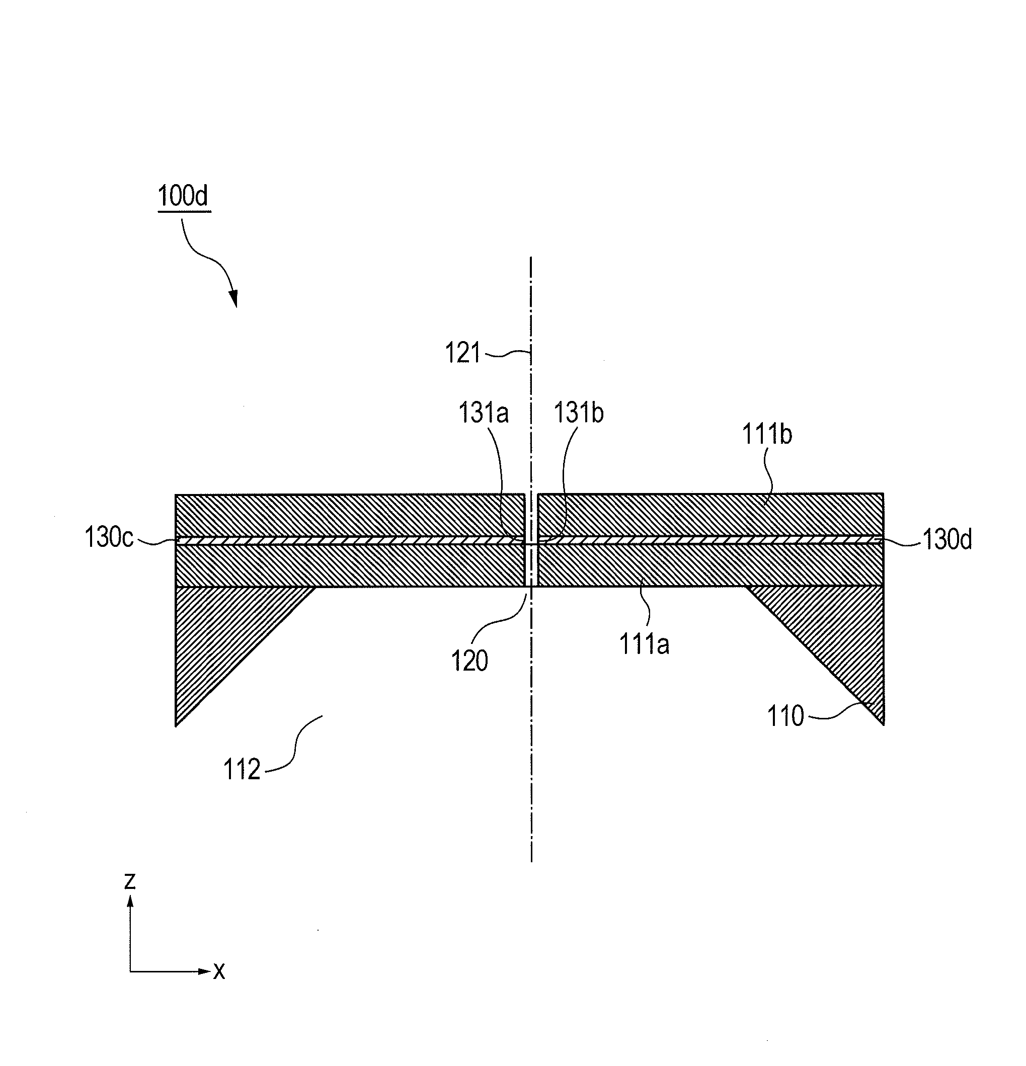
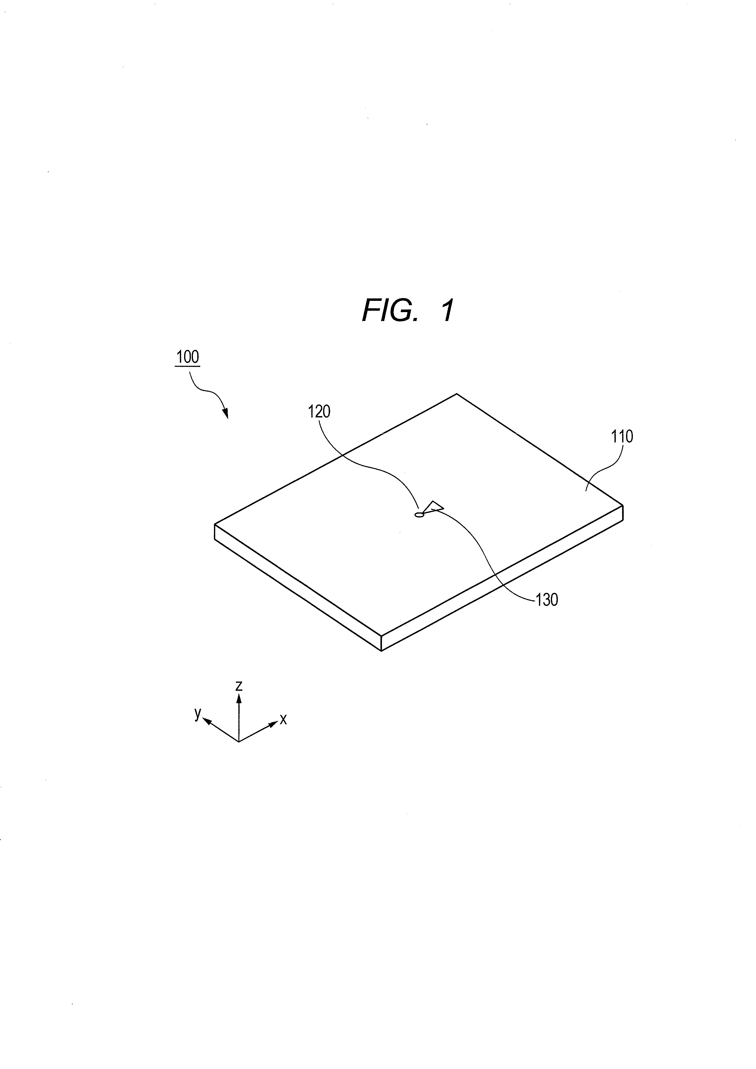
[0073]An example of the construction of a nanopore chip for analyzing the characteristics of a biopolymer of the present invention will be described referring to FIG. 1. FIG. 1 is a schematic diagram of a nanopore chip 100 for analyzing the characteristics of a biopolymer according to this embodiment of the present invention. As shown in the figure, the nanopore chip 100 is composed a substrate 110, a nanopore 120, and an electroconductive thin film 130, or the like. As shown in FIG. 1, a plane parallel to a widest plane (hereinafter, simply referred to as a substrate surface) of the substrate 110 is defined as a x-y plane, a direction, in which an electroconductive thin film 130 and the nanopore 120 are aligned, is defined as a x axis, and a direction perpendicular to the x-y plane is defined as a z axis. The nanopore 120 is formed approximately perpendicularly to the substrate surface; namely, the central axis of the nanopore ...

second embodiment

Multinanopore Analysis Device Construction

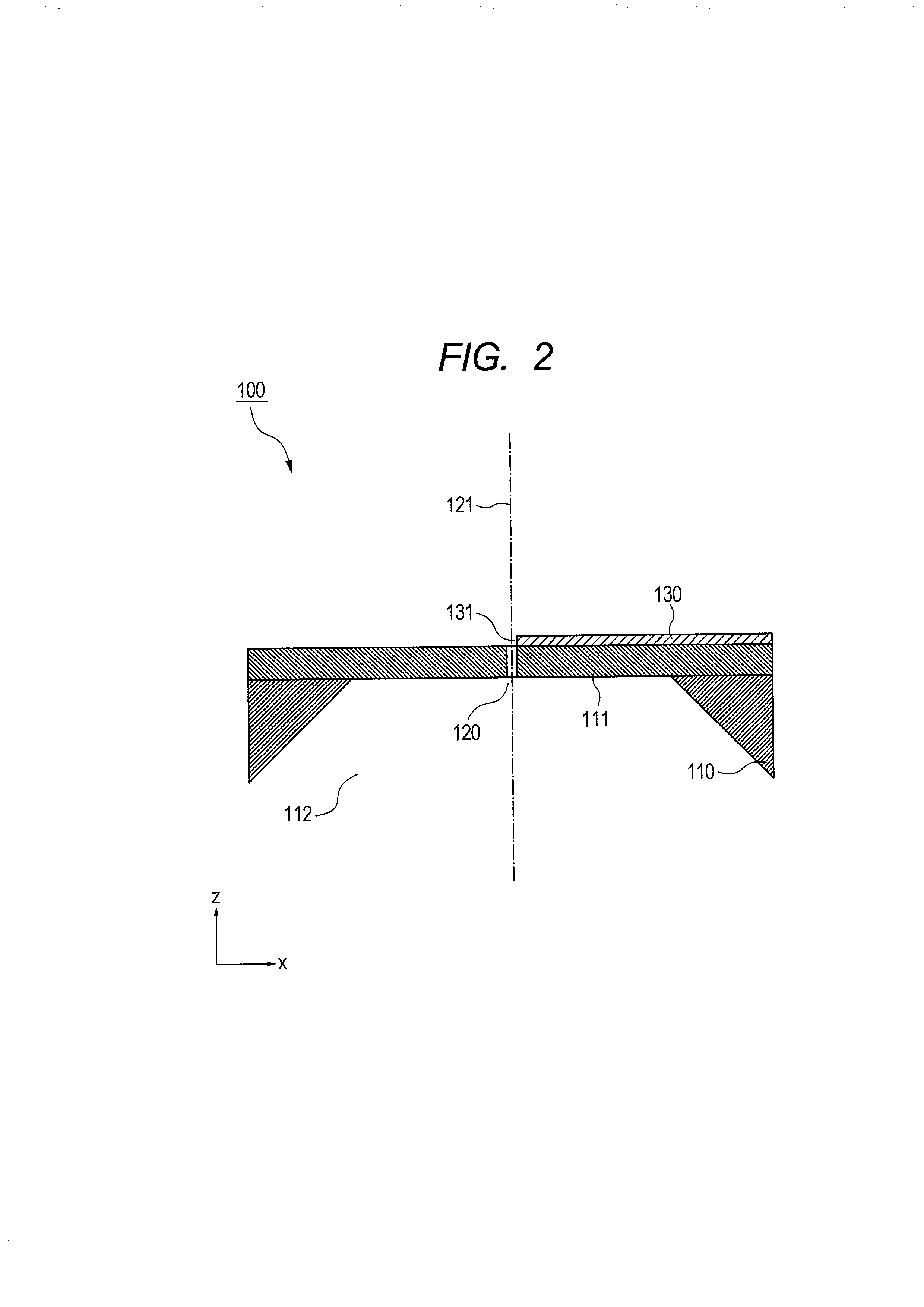
[0111]One example of the construction of a multinanopore chip for biopolymer property analysis according to the second embodiment of the present invention will be described referring to FIG. 11. FIG. 11 is a schematic diagram of the multinanopore chip 1100 for biopolymer property analysis according to the second embodiment. As shown in the figure, the nanopore chip 1100 is composed of a substrate 1110, nanopores 1120, 1121, and electroconductive thin films 1130a, 1130b, 1131a, and 1131b, or the like. As shown in the figure, the multinanopore chip 1100 according to this embodiment has a plurality of unit structures composed of nanopores and electroconductive thin films facing to each other, or the like, according to the aforementioned variation, namely the unit structures shown in FIG. 10, on a single substrate 1110.

[0112]Next, one example of the construction of the biopolymer property analysis device according to this embodiment will be desc...


PUM

PropertyMeasurementUnit
thicknessaaaaaaaaaa
sizeaaaaaaaaaa
sizeaaaaaaaaaa

Abstract

The present invention provides a device and method for analyzing the characteristics of a biopolymer with excellent mechanical stability, high spatial resolution and sensitivity using a simple device construction. Specifically, the Raman scattered light of a biopolymer is measured and the properties of monomer units forming the biopolymer are analyzed by using a biopolymer property analysis chip (100a) characterized by comprising: a solid substrate (110); at least one nanopore (120) disposed in the solid substrate (110); and one or more electrically conductive thin films (130a, 130b) disposed on the solid substrate (110). The biopolymer property analysis chip (100a) is characterized in that the electrically conductive thin films (130a, 130b) are disposed partially on the solid substrate (110) where the nanopore (120) is formed and a biopolymer which has penetrated into the nanopore (120) is caused to generate Raman scattered light by means of irradiation with external light.

Description

TECHNICAL FIELD[0001]The present invention relates to a device and method for analyzing the characteristics of a biopolymer by using an analysis chip with a nano-sized pore (hereinafter, simply referred to as a “nanopore”) formed thereon. The present invention in particular relates to a device and method for analyzing biopolymer properties characterized in that a near field is formed on the nanopore chip to detect biopolymers such as nucleic acid optically without the need for labeling.BACKGROUND ART[0002]Techniques using nanopores attract tremendous attentions as an approach to the implementation of post-Next-Generation DNA sequencers. It is considered that the nanopore techniques have a noteworthy advantage in that they allow the characteristics of a biopolymer to be analyzed without DNA labeling, namely using no reagents, such as an enzyme and fluorescent dye. The nanopores may be largely classified into two types. One is a so-called bionanopore, of which channel protein forming ...

Claims


Application Information

Patent Timeline
Patent Type & Authority Applications(United States)
IPC IPC(8): G01J3/02
CPCB82Y5/00B82Y15/00G01N21/658G01J3/0267G01N33/48721C12Q1/6869C12Q2565/631C12Q2565/632
Inventor OZAWA, SATOSHIANAZAWA, TAKASHIAKAHORI, RENATAKAHASHI, SATOSHIOHURA, TAKESHIKIGUCHI, MASASHI
Owner HITACHI HIGH-TECH CORP
Why Eureka
Try Eureka