Hybrid substrate, production method therefor, and semiconductor integrated circuit package

a technology of hybrid substrates and integrated circuits, which is applied in the direction of resistive material coating, printed circuit simultaneous processing, solid-state devices, etc., can solve the problems of hard to sintered ceramic substrates in cases with large sizes, solder connections can come off substrates, and the effect of effective absorption of stress

Active Publication Date: 2013-08-08
PANASONIC INTELLECTUAL PROPERTY MANAGEMENT CO LTD
View PDF3 Cites 22 Cited by
  • Summary
  • Abstract
  • Description
  • Claims
  • Application Information

AI Technical Summary

Benefits of technology

[0039]In the hybrid substrate according to the present invention, the core layer portion of the substrate has a sintered integration structure composed of the glass woven cloth and the glass-ceramic sintered body, the glass woven cloth being functioning as the reinforcing material and the glass-ceramic sintered body being formed by the impregnation of the glass woven cloth. Thus, the hybrid substrate of the present invention as a whole can be suitably treated as a large-sized single substrate. In this regard, the hybrid substrate of the present invention can have a large principal surface whose size is 255-600 mm×255-600 mm, for example.
[0040]Even if the hybrid substrate is formed into a large-sized thin substrate according to the present invention, the glass woven cloth serving as the reinforcing material can fulfill a role of keeping the whole substrate strong, and thereby an occurring of a cracking, a breaking and the like of the substrate can be suppressed.
[0041]The glass woven cloth as the reinforcing material also fulfills a role of effectively absorbing a stress which may be possibly exerted on the glass-ceramic sintered body. Thus, even when the hybrid substrate of the present invention is formed thinner and larger and also

Problems solved by technology

Under such a current situation that the down-sizing and the increase in the number of I/O terminals is coincidentally developing, the down-sizing of terminal pitches and/or narrower pitching of the terminals is further developing, which causes a difficulty in a mounting of a semiconductor integrated circuit (i.e., LSI) on a packaged circuit board.
In the course of more use of large-sized chips, such a problem may arise that a solder connection can come off the substrate due to a substrate warpage occurred during a manufacturing process thereof, or due to a substrate warpage attributed to a thermal history upon a LIS chip mounting

Method used


Image

  • Hybrid substrate, production method therefor, and semiconductor integrated circuit package
  • Hybrid substrate, production method therefor, and semiconductor integrated circuit package
  • Hybrid substrate, production method therefor, and semiconductor integrated circuit package

Examples


first embodiment

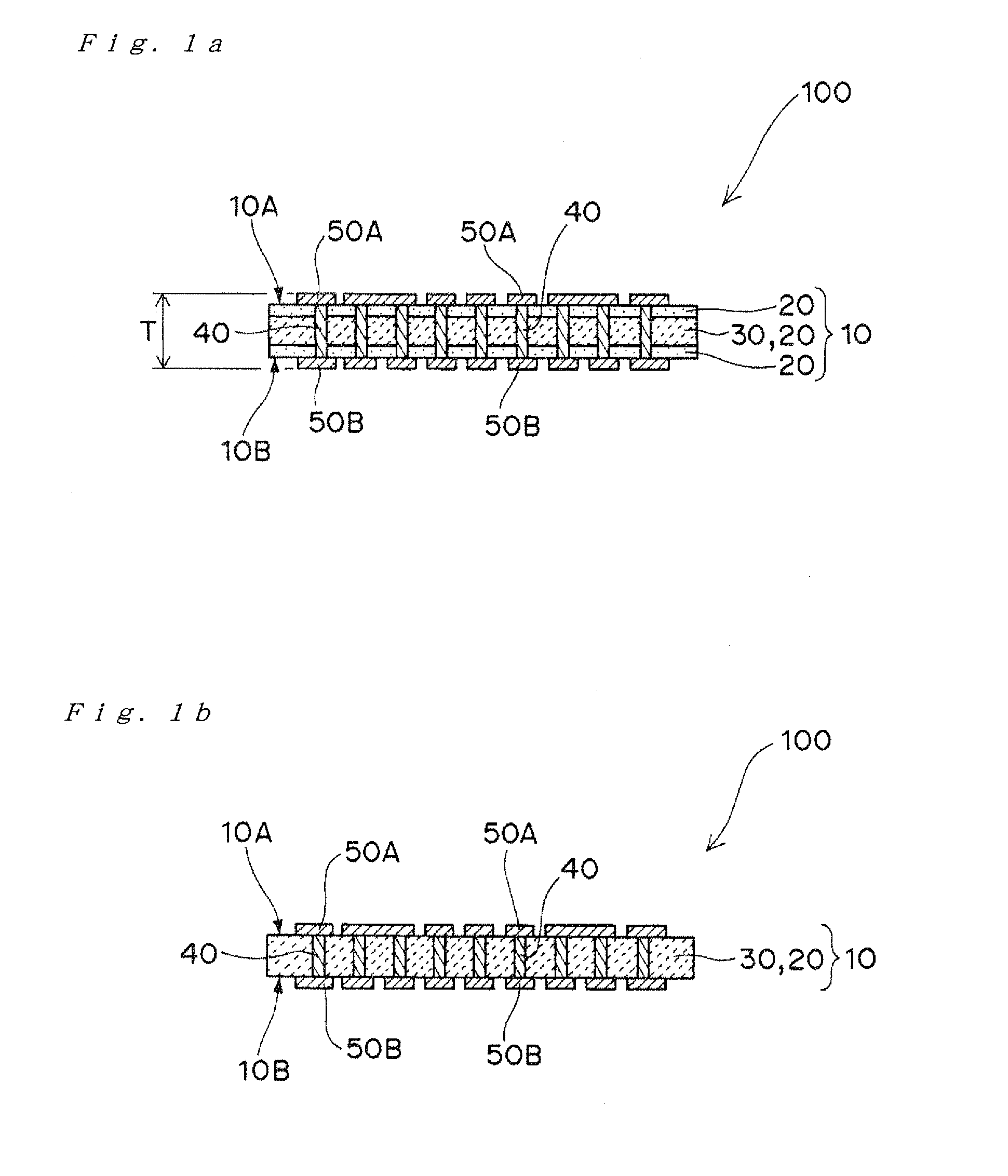
[0063]A hybrid substrate 100 of the present invention comprises, as illustrated in FIGS. 1(a) and 1(b), a glass-ceramic sintered body 20 and a glass woven cloth 30 existing therein. The glass-ceramic sintered body 20 and the glass woven cloth 30 provide a core layer 10 of the substrate 100. Specifically, the core layer of the hybrid substrate 100 comprises the glass woven cloth 30 serving as a reinforcing material, and the “glass-ceramic sintered body 20 which at least contains a glass component and a metal oxide component” obtained by an impregnation of the glass woven cloth. Particularly according to the present invention, the glass woven cloth 30 and the glass-ceramic sintered body 20 formed by the impregnation with respect to the glass woven cloth 30 are in a form of sintering integration with each other in the core layer 10 of the hybrid substrate.

[0064]As illustrated in FIG. 1, the hybrid substrate 100 according to the first embodiment comprises a through-hole 40 passing throu...

second embodiment

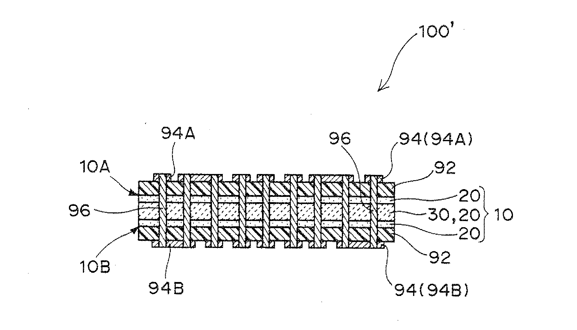
[0078]The present invention makes it possible to embody the various configurations of the hybrid substrate which comprises the core layer including the glass woven cloth and the glass-ceramic sintered body integrated together by sintering. For example, the configuration of a hybrid substrate 100′ as illustrated in FIGS. 6(a) and 6(b) can be possible according to the present invention. As illustrated in FIGS. 6(a) and 6(b), the hybrid substrate 100′ comprises thermoset insulating resin layers 92 on both opposed surfaces 10A, 10B of the “core layer 10 comprising the glass woven cloth 30 and the glass-ceramic sintered body 20 existing in and / or on the glass woven cloth 30”. The thermoset insulating resin layers 92 are provided with the wiring layers 94 thereon. Further, through-hole 96 is provided so as to pass through the core layer 10 and the thermoset insulating resin layers 92 in the hybrid substrate 100′.

[0079]Even in the case of the hybrid substrate 100′ as illustrated in FIGS. 6...


PUM

PropertyMeasurementUnit
Diameteraaaaaaaaaa
Diameteraaaaaaaaaa
Sizeaaaaaaaaaa

Abstract

A hybrid substrate according to the present invention comprises a core layer composed of a glass woven cloth as a reinforcing material, and a glass-ceramic sintered body which at least comprises a glass component and a metal oxide component. The glass woven cloth and the glass-ceramic sintered body formed by an impregnation with respect to the glass woven cloth are in a form of sintering integration with each other.

Description

TECHNICAL FIELD[0001]The present invention relates to a hybrid substrate, a manufacturing method for the hybrid substrate, and also a semiconductor integrated circuit package. More particularly, the present invention relates to a hybrid substrate whose core layer is made of different materials, and also a method for manufacturing such hybrid substrate. The present invention also relates to a semiconductor integrated circuit package which is obtainable from the hybrid substrate.BACKGROUND OF THE INVENTION[0002]With the development of the electronic equipment, a semiconductor integrated circuit employed in a CPU of a computer and a digital television has been improved in terms of its processing speed. Particularly, an image processing LSI is developing in terms of an increasing processing speed, and also a further integration is advanced. There is also a demand for a down-sizing and an increase in the number of I / O terminals.[0003]Under such a current situation that the down-sizing an...

Claims


Application Information

Patent Timeline
IPC IPC(8): H05K1/03H05K3/10H01L23/498
CPCH01L23/15H01L23/49827H01L2924/09701H01L2924/12044H05K3/4605H05K2201/029H01L21/4857H05K1/0306H05K3/107H01L2224/16225H05K3/0097H05K2203/1126H01L23/49822H01L23/49811
Inventor NAKATANI, SEIICHIKAWAKITA, KOJI
Owner PANASONIC INTELLECTUAL PROPERTY MANAGEMENT CO LTD
Why Eureka
Try Eureka