Ferromagnetic Tunnel Junction Structure and Magnetoresistive Effect Device and Spintronics Device Utilizing Same

a tunnel junction and magnetoresistive effect technology, applied in the direction of magnetic field-controlled resistors, semiconductor devices, galvano-magnetic material selection, etc., can solve the problems of low resistance of the mtj device, generation of defects such as mgo barrier dislocation, and low tmr value, so as to suppress the deterioration of the element during the device processing process, reduce the mismatch of the lattice, and reduce the tmr value

Active Publication Date: 2013-08-29
NAT INST FOR MATERIALS SCI
View PDF1 Cites 113 Cited by
  • Summary
  • Abstract
  • Description
  • Claims
  • Application Information

AI Technical Summary

Benefits of technology

[0035]According to the present invention, the use of disordered spinel structure in which arrangement of atoms (for example, Mg atoms and Al atoms) are disordered provides TMR value that is larger than the case of using ordered spinel barrier (for example, MgAl2O4 spinel barrier). In addition, tunnel barrier and tunnel junction with qualities higher than the case of using MgO barrier can be obtained by sputtering method. Further, the disordered structure allows preparation of the tunnel barrier layer within wide range of composition. For example, the lattice constant can be modulated in the composition defined by MgxAl(0.4-0.8x)O(0.6-0.2x), where 0≦x<½ is satisfied. As a result, it is possible to reduce the lattice mismatch in the interface with the adjacent ferromagnetic layer to a minimum level. By this constitution, it is possible to maintain a high TMR value even when a high bias voltage is applied.
[0036]Different from the perfectly ionic crystal of MgO, the disordered spinel is free of deliquescency and is chemically stable due to the covalent bond (for example, generated by the presence of Al). Therefore, it is possible to suppress deterioration of the element during device processing process. Therefore, the tunnel junction structure of the present invention can be applied to magnetic head of hard disk drive (HDD), MRAM, and to various spin electronics device such as a spin resonance tunnel device constituted of ferromagnetic dual tunnel junction, and spin logic device such as spin MOSFET requiring effective spin injection to the semiconductor, each requiring application of bias voltage. Specifically, when a magnetic layer is stacked on Si substrate or Ge substrate via a tunnel barrier layer in the application to spin MOSFET, the use of non-magnetic material according to the invention having the disordered spinel structure such as disordered Mg—Al—O as the barrier layer, it is possible to grow a magnetic layer with small lattice strain. As a result, it is possible to inject spins from the magnetic layer to the Si or Ge effectively. In addition, similar effect can be expected in the disordered spinel based material having constituent elements other than Mg and Al. Thus, the disordered spinel may be combined with various ferromagnetic, nonmagnetic materials.

Problems solved by technology

In addition, an MTJ device of low resistance is required due to the increasing importance of spin transfer magnetization switching, where magnetization of the MTJ device is switched by injection of spin polarized current.
Under the above-explained circumstance, the conventional AlOx amorphous barrier is not appropriate for the spin electronics device because of a too large contact resistance, heterogeneous properties due to large interface roughness between the ferromagnetic layer and the barrier layer, and generally small TMR value of about several tens % at room temperature.
However, where the Co-based full Heusler alloy is used as a material of ferroelectric layer, tunnel junction of high quality cannot be obtained due to large lattice mismatches with MgO (for example, Co2FeSi and MgO shows mismatch of 6%), resulting in generation of defects such as dislocations in the MgO barrier (H. Sukegawa et al., Phys. Rev. B 79, 184418 (2009)).
Specifically, Co-based full Heusler alloy grown on the MgO barrier tends to have a disordered structure, and a large TMR value expected from half-metal is not detected.
As a result, the theoretically simulated enhancement of TMR due to the coherent tunnel effect is not always observed.
However, in the MTJ device having the amorphous AlOx barrier or the MgO barrier, there has been a general problem of reduction of TMR value to half of the zero-bias value upon application of bias voltage of about 500 mV.
The large bias-voltage dependence of the TMR value is mainly caused by lattice defects and interface roughness between the ferromagnetic layer and the barrier layer.
In the conventional amorphous AlOx barrier or MgO having large lattice misfit, it is very difficult to improve the above-described bias voltage dependence.
However, the obtained TMR value was not sufficiently large in comparison with crystalline MgO, and improvement was required.

Method used


Image

  • Ferromagnetic Tunnel Junction Structure and Magnetoresistive Effect Device and Spintronics Device Utilizing Same
  • Ferromagnetic Tunnel Junction Structure and Magnetoresistive Effect Device and Spintronics Device Utilizing Same
  • Ferromagnetic Tunnel Junction Structure and Magnetoresistive Effect Device and Spintronics Device Utilizing Same

Examples


example 1

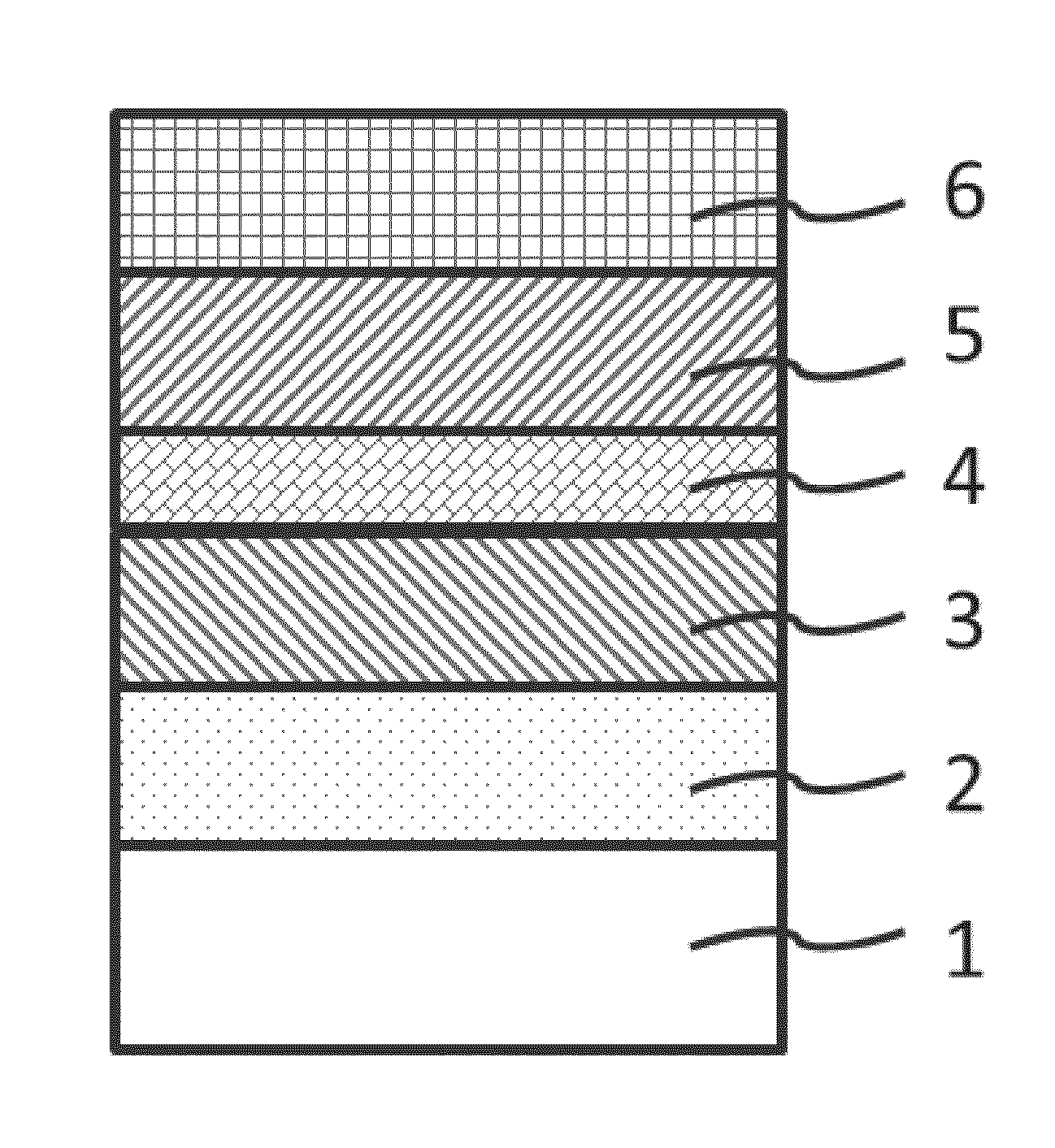
[0071]Under room temperature, a Cr layer of 40 nm in thickness and Fe layer of 30 nm in thickness were sequentially stacked on a MgO (001) substrate using a magnetron sputtering device, where the Cr layer was formed as a buffer layer. After that, the substrate was subjected to heat treatment at 200° C. for 15 minutes to improve crystallinity of the Fe film. Next, Mg film of 0.45 nm was formed at room temperature. The obtained stacked film (stacked structure) of MgO (001) substrate / Cr (40 nm) / Fe (30 nm) / Mg (0.45 nm) was introduced into a chamber for oxidation. Mg33Al67 layer of 1.5 nm was formed on the Mg layer by sputtering a target having Mg33Al67 alloy composition. Ar and oxygen were introduced into the chamber, and Mg—Al oxide film was formed by induced plasma coupling (ICP) treatment. In this treatment, the ratio of the partial pressures of Ar and oxygen was 3:17, the total gas pressure was 6 Pa, and the duration of oxidation was 15 seconds.

[0072]The stacked film was introduced ...

example 2

[0091]Except for the target composition of Mg17Al83, using the same method as Example 1, MTJ device of Cr (40 nm) / Fe (30 nm) / Mg (0.45 nm) / Mg17Al83 (0.9 nm)-O / Fe (7 nm) / IrMn (12 nm) / Ru (7 nm) structure was prepared, where “Mg (0.45 nm) / Mg17Al83 (0.9 nm)-O” denotes an Mg—Al—O layer that was formed by oxidation of Mg layer of 0.45 nm and Mg17Al83 layer of 0.9 nm stacked on the Mg layer.

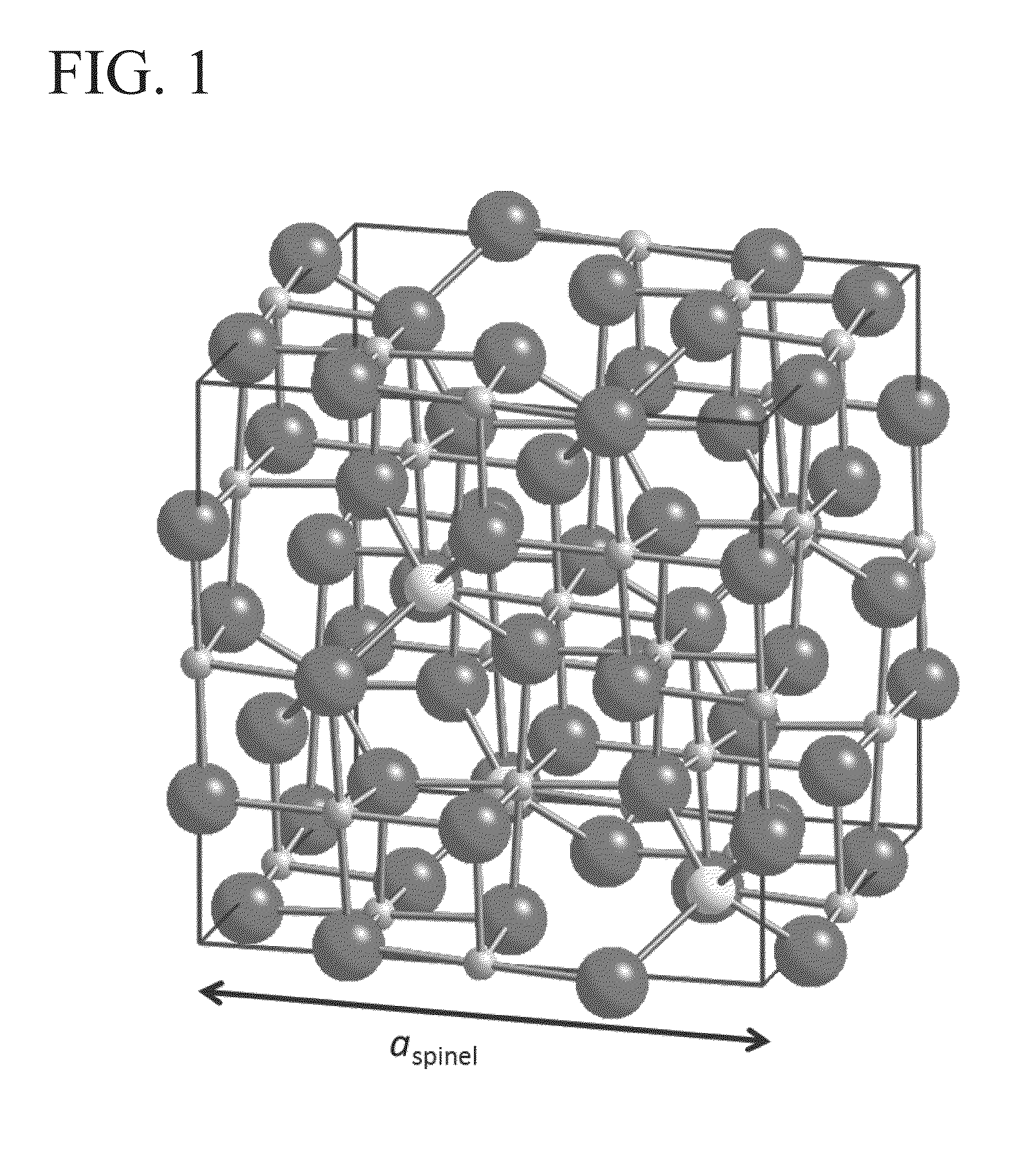
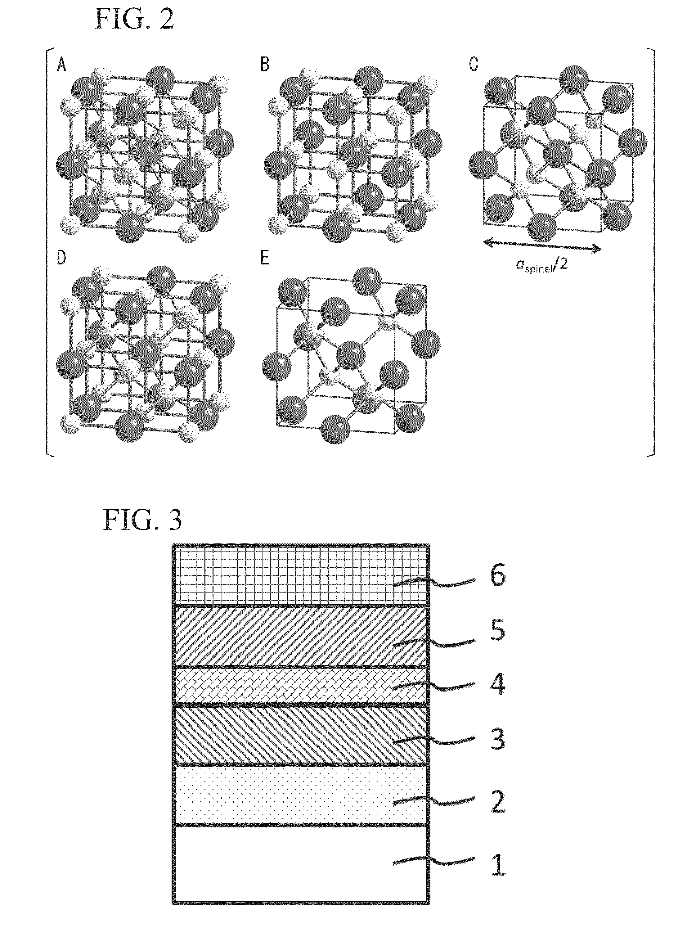
[0092]It was confirmed that the Mg—Al—O layer had a disordered spinel structure like as Example 1. Because of the large Al amount, the lattice constant of Mg—Al—O was further reduced, and the in-plane lattice mismatch of the barrier layer and the Fe layer in the obtained junction was as low as 0.1%.

[0093]Large TMR value was obtained such that TMR value at 15K was 304%, and TMR value at room temperature was 185%. Along with realization of the high lattice matching, as shown in FIG. 7, Vhalf showed large value of 1400 mV at positive bias voltage, and 1200 mV at negative bias voltage. Here, positive bias is...

example 3

[0094]Except for forming a CoFe alloy layer between the upper and lower magnetic layers and the barrier layer, according to the same manner as Example 1 and Example 2, an MTJ having Cr (40 nm) / Fe (30 nm) / Co50Fe50 (2.5 nm) / Mg (0.45 nm) / Mg33Al67 (0.9 nm)-O / Co50Fe50 (2.0 nm) / Fe (5 nm) / IrMn (12 nm) / Ru (7 nm) was produced. CoFe alloy has a bcc structure and substantially same lattice constant with Fe. Therefore, CoFe layer inserted between the Fe layer and the barrier layer was also grown epitaxially. Since spin polarization of CoFe alloy is larger than that of pure Fe, TMR values at 15K and at room temperature were largely increased to 479% and 308% compared to the case of using Fe.


PUM


Abstract

A ferromagnetic tunnel junction structure comprising a first ferromagnetic layer, a second ferromagnetic layer, and a tunnel barrier layer that is interposed between the first ferromagnetic layer and the second ferromagnetic layer, wherein the tunnel barrier layer includes a crystalline non-magnetic material having constituent elements that are similar to those of an crystalline oxide that has spinel structure as a stable phase structure; the non-magnetic material has a cubic structure having a symmetry of space group Fm-3m or F-43m in which atomic arrangement in the spinel structure is disordered; and an effective lattice constant of the cubic structure is substantially half of the lattice constant of the oxide of the spinel structure.

Description

BACKGROUND OF THE INVENTION[0001]1. Field of the Invention[0002]The present invention relates to a ferromagnetic tunnel junction structure constituted of a tunnel barrier layer and two ferromagnetic layers that sandwiches the tunnel barrier layer, and application of the same structure to a magnetoresistive effect device and to spintronics devices. Priority is claimed on Japanese Patent Application No. 2012-039582 filed on Feb. 27, 2012, the content of which is incorporated herein by reference.[0003]2. Description of Related Art[0004]In recent years, giant magnetoresistance (GMR) effect device constituted of multilayers of ferromagnetic layer / nonmagnetic metal layer, and ferromagnetic tunnel junction (MTJ) device constituted of ferromagnetic layer / insulation layer (tunnel barrier layer, barrier layer) / ferromagnetic layer have been paid much attentions to as novel devices for magnetic field censors and nonvolatile random access magnetic memories (MRAM). Known types of GMR includes cur...

Claims


Application Information

Patent Timeline
Patent Type & Authority Applications(United States)
IPC IPC(8): H01L29/82
CPCH01L43/08H01L27/228H01L43/10H10N50/10H10N50/85H10B61/22
Inventor SUKEGAWA, HIROAKIMITANI, SEIJINIIZEKI, TOMOHIKOOHKUBO, TADAKATSUINOMATA, KOUICHIROHONO, KAZUHIROSHIRAI, MASAFUMIMIURA, YOSHIOABE, KAZUTAKAMURAMOTO, SHINGO
Owner NAT INST FOR MATERIALS SCI
Why Eureka
Try Eureka