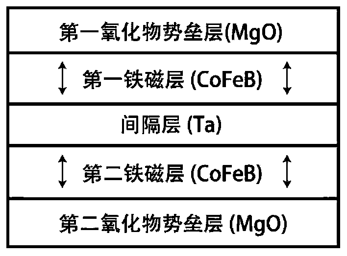
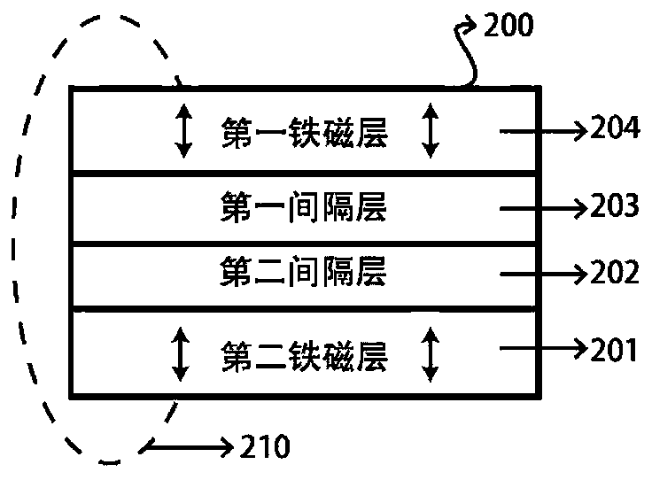
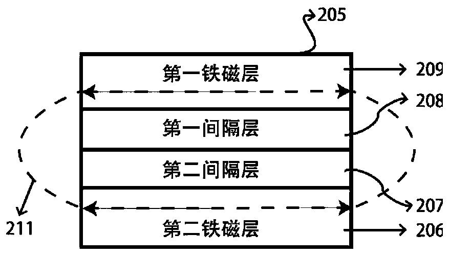
A multilayer film with double spacer layers that can form ferromagnetic or antiferromagnetic coupling
A technology of antiferromagnetic coupling and ferromagnetic layer, applied in the fields of non-volatile magnetic memory and magnetic logic, which can solve the problems of increased magnetic damping coefficient, inability to generate, strong perpendicular magnetic anisotropy, etc.
- Summary
- Abstract
- Description
- Claims
- Application Information
AI Technical Summary
Problems solved by technology
Method used
Image
Examples
Embodiment 1
[0035] image 3 Shown is a schematic structural diagram of the present invention as a free layer in a perpendicular magnetic anisotropic magnetic tunnel junction. During the fabrication process, the buffer layer 302 is firstly deposited on the substrate 301 , followed by the pinning layer 303 , the reference layer 304 , the second oxide barrier layer 305 , the free layer 308 and the capping layer 307 . In some embodiments, the buffer layer 302 is a Ta / Ru / Ta multilayer film, which is used to reduce surface roughness while promoting the formation of the growth crystal direction of the ultra-thin multilayer film; the pinning layer 303 is a Co / Pt multilayer film , used to fix the magnetization direction of the reference layer; the reference layer 304 is Co 20 Fe 60 B 20 , with a thickness of 1.3nm, whose magnetization direction is fixed by the pinning layer for reference; the material of the second oxide barrier layer 305 is MgO, with a thickness of 0.9nm, for providing tunneli...
Embodiment 2
[0038] Figure 4 Shown is a schematic structural diagram of the present invention as a free layer in an in-plane magnetic anisotropic magnetic tunnel junction. During the fabrication process, the buffer layer 402 is firstly deposited on the substrate 401 , followed by the pinning layer 403 , the reference layer 404 , the second oxide barrier layer 405 , the free layer 408 and the capping layer 407 . In some embodiments, the buffer layer 402 is a Ta / Ru / Ta multilayer film, which is used to reduce the surface roughness and at the same time promote the formation of the growth crystal direction of the ultrathin multilayer film; Magnetic material for fixing the magnetization direction of the reference layer; the reference layer 404 is Co 20 Fe 60 B 20 , with a thickness of 2.5nm, whose magnetization direction is fixed by the pinning layer for reference; the material of the second oxide barrier layer 405 is MgO, with a thickness of 0.9nm, for providing tunneling effect; the free l...
Embodiment 3
[0041] Figure 5 Shown is a schematic structural diagram of the present invention as a reference layer in a perpendicular magnetic anisotropy magnetic tunnel junction. During the fabrication process, the buffer layer 502 is firstly deposited on the substrate, followed by the pinning layer 503 , the reference layer 508 , the first oxide barrier layer 505 , the free layer 506 and the capping layer 507 . In some embodiments, the buffer layer 502 is a Ta / Ru / Ta multilayer film, which is used to reduce surface roughness while promoting the formation of the growth crystal direction of the ultra-thin multilayer film; the pinning layer 503 is a Co / Pt multilayer film , used to fix the magnetization direction of the reference layer; the reference layer 508 is composed of a second oxide barrier layer 504 structure and a multilayer film structure 200 that can exhibit perpendicular magnetic anisotropy, wherein the second oxide barrier layer 504 material is MgO, the thickness is 0.9nm; the ...
PUM
| Property | Measurement | Unit |
|---|---|---|
| thickness | aaaaa | aaaaa |
| thickness | aaaaa | aaaaa |
| thickness | aaaaa | aaaaa |
Abstract
Description
Claims
Application Information


