Athermal Photonic Waveguide With Refractive Index Tuning

a photonic waveguide and refractive index technology, applied in the field of photonic waveguides, can solve the problems of temperature excursions that can prove problematic for silicon-based photonics, failure to achieve the production and operation of such platforms, and impose severe process constraints on integrated photonic devices. achieve the effect of reducing the need for active power-consuming compensation techniques

Active Publication Date: 2013-09-19
POLITECNICO DI MILANO +1
View PDF3 Cites 23 Cited by
  • Summary
  • Abstract
  • Description
  • Claims
  • Application Information

AI Technical Summary

Benefits of technology

[0010]With this waveguide arrangement, there is provided permanent tuning of the effective index of the waveguide without changing the thermo-optic behavior of the waveguide. As a result, there is achieved both passive athermal operation with post-fabrication refractive index tuning of the waveguide structure. This index tuning provides complete compensation for microfabrication tolerances and enables the realization of tight design specifications; and with the use of photo-sensitive tuning materials, enables permanently reconfigurable devices, eliminating the need for active, power-consuming compensation techniques. The passive athermal operation produced by the TO compensation cladding layer is obtained with near complete thermo-optic compensation, eliminating the need for active temperature control. Together, these functionalities enable a wide range of photonic systems for which photonic-electronic integration is required. Other features and advantages will be apparent from the following description and accompanying figures, and from the claims.

Problems solved by technology

In the development of densely integrated silicon-based electronic-photonic device platforms, there have been discovered two significant challenges to the successful production and operation of such platforms.
Thus, even for the most advanced and highly accurate microfabrication processes, integrated photonic device requirements impose a severe process constraint, especially for resonant devices, as well as multi-stages and high-quality-factor devices.
Secondly, it is found that during the operation of densely-integrated electronic-photonic platforms, there can be produced significant local as well as global temperature excursions across the platform, e.g., a CMOS chip, and that such temperature excursions can prove problematic for silicon-based photonics.
In particular, variations in the thermo-optic (TO) index of photonic materials can induce temperature-dependent wavelength shifts (TDWS) of, e.g., resonant photonic devices, that can limit wavelength resolution in important photonic applications such as WDM, high-resolution spectroscopy, and other applications.
With these limitations, there remain significant challenges to achieving the functionality and operational performance required of monolithically-integrated electronic-photonic device platforms.
Successful electronic-photonic integration on a CMOS platform cannot be fully realized without the achievement of such.

Method used


Image

  • Athermal Photonic Waveguide With Refractive Index Tuning
  • Athermal Photonic Waveguide With Refractive Index Tuning
  • Athermal Photonic Waveguide With Refractive Index Tuning

Examples


example i

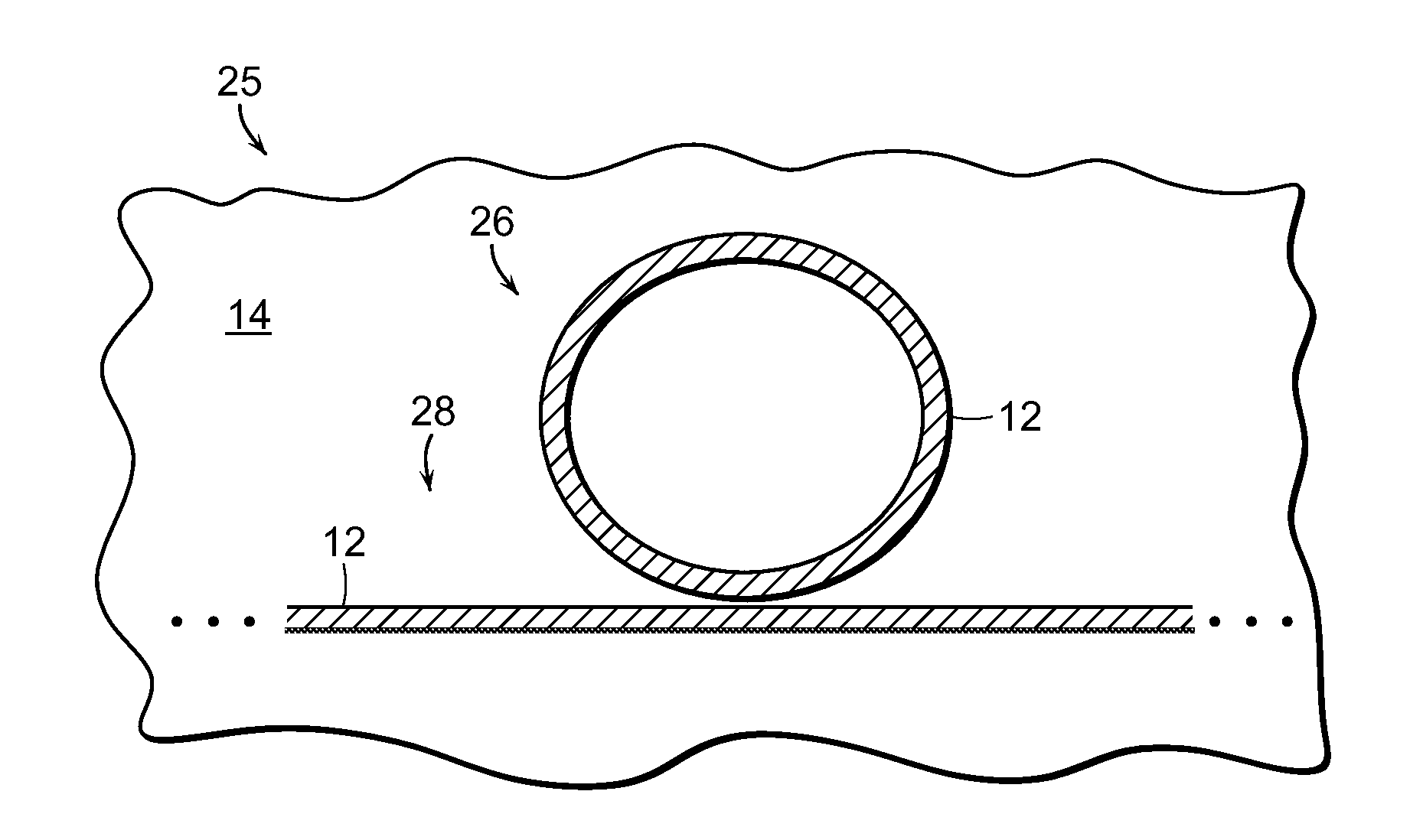
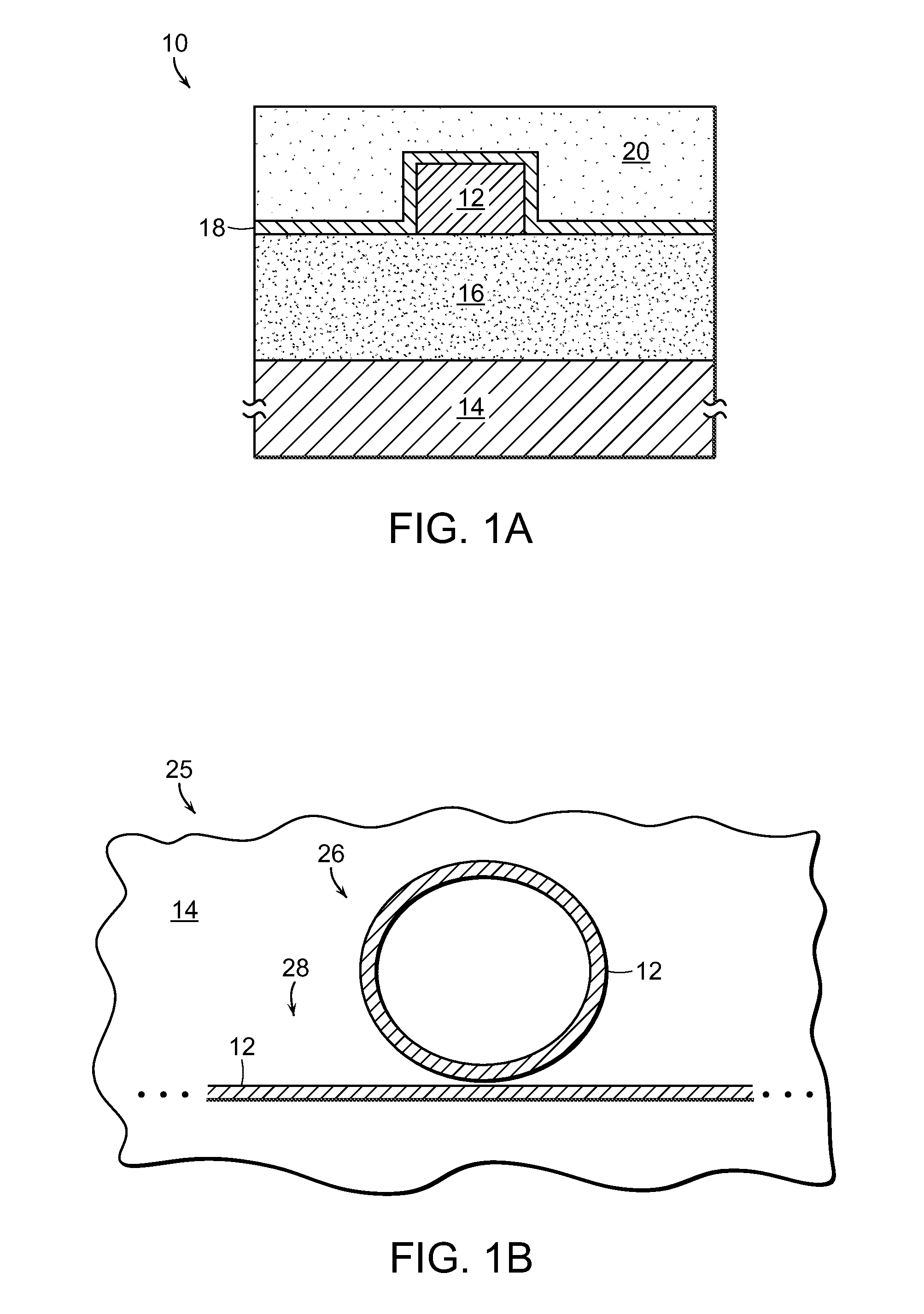
[0054]The waveguide structure of FIG. 1A was microfabricated as a racetrack resonator structure as in FIG. 1B. The closed loop 26 of the resonator had a bending radius of 20 μm and was disposed adjacent to a bus waveguide 28, with a coupling length of 100 μm and a gap of 600 nm in the coupling section. The waveguide structure was microfabricated with an amorphous waveguide core of 500 nm×205 nm and 205 nm in thickness, on a 3 μm-thick SiO2 undercladding layer, atop a silicon substrate. A photo-sensitive refractive index tuning cladding layer of As2S3, with 50 nm in thickness, was provided on the waveguide core, and a TO compensation cladding layer of the commercially available polymer EP, from Enablence, Inc., with 3 μm in thickness was provided on the index tuning cladding layer. The structure was annealed in the manner described above.

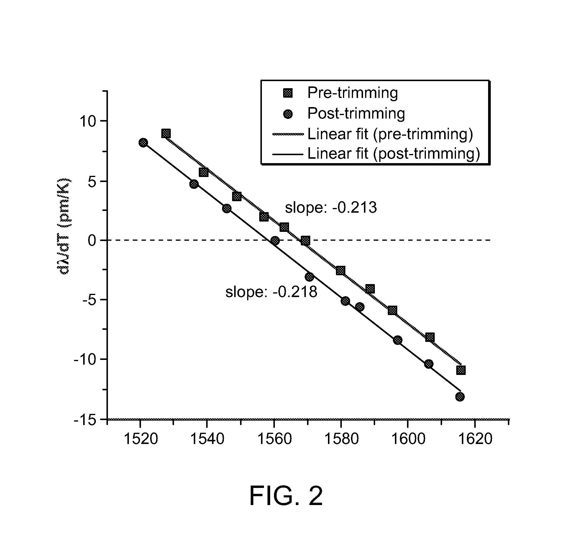
[0055]The operation of the resulting photonic device was investigated before and after exposing the structure to illumination to tune the refractive...

example ii

[0058]The rate of refractive index tuning of the photo-sensitive chalcogenide As2S3 was investigated. Three refractive index cladding layers of As2S3 were separately formed, having thicknesses of 20 nm, 30 nm, and 50 nm on the waveguide structure of FIGS. 1A-1B. The devices with various thicknesses of As2S3 were to visible light radiation from a halogen lamp that was coupled to an optical fiber controllably disposed on the material. The magnitude of each device's resonant wavelength change induced by the photo-induced refractive index change was examined as a function of exposure time. FIG. 3 is a plot of such for each of the three different material thickness devices. As seen by the plot, the magnitude of wavelength change is higher for a thinner As2S3 for a given exposure time. In other words, the magnitude of index change is inversely proportional to the thickness, where ΔnAs2S3 / nAs2S3=×tAs2S3 / tAs2S3 for a given exposure dosage. The observed blue-shift in the resonance wavelength...


PUM


Abstract

In a photonic waveguide, there is provided an undercladding layer and a waveguide core, having a cross-sectional height and width, that is disposed on the undercladding layer. The waveguide core comprises a waveguide core material having a thermo-optic coefficient. A refractive index tuning cladding layer is disposed on top of the waveguide core. The refractive index tuning cladding layer comprises a refractive index tuning cladding material having an adjustable refractive index and an absorption length at a refractive index tuning radiation wavelength. A thermo-optic coefficient compensation cladding layer is disposed on top of the refractive index tuning cladding layer. The thermo-optic coefficient compensation cladding layer comprises a thermo-optic coefficient compensation material having a thermo-optic coefficient that is of opposite sign to the thermo-optic coefficient of the waveguide core material. The thermo-optic coefficient compensation cladding layer provides at least partial compensation for the waveguide core thermo-optic coefficient.

Description

CROSS-REFERENCE TO RELATED APPLICATIONS[0001]This application claims the benefit of U.S. Provisional Application No. 61 / 597,382, filed Feb. 10, 2012, the entirety of which is hereby incorporated by reference.STATEMENT REGARDING FEDERALLY SPONSORED RESEARCH[0002]This invention was made with Government support under Grant No. HR0011-10-0-0009, awarded by the Defense Advanced Research Projects Agency. The Government has certain rights in the invention.BACKGROUND[0003]This invention relates generally to photonic waveguides, and more particularly relates to techniques for compensation of both microfabrication variation and operational thermal fluctuations in photonic waveguides.[0004]The increasing demand for reduction in electronics power consumption, together with the increasing demand for communication bandwidth, has led to a photonic system paradigm based on the dense monolithic integration of electronic and photonic devices. In this paradigm, the integrated electronics provide compu...

Claims


Application Information

Patent Timeline
Patent Type & Authority Applications(United States)
IPC IPC(8): G02B6/036G02B6/02
CPCG02B6/02033G02B6/122G02B6/03694
Inventor AGARWAL, ANURADHA M.CANCIAMILLA, ANTONIOMORICHETTI, FRANCESCOGRILLANDA, STEFANOKIMERLING, LIONEL C.MELLONI, ANDREAMICHEL, JURGENRAGHUNATHAN, VIVEKSINGH, VIVEK
Owner POLITECNICO DI MILANO
Why Eureka
Try Eureka