Supercharge Your Innovation With Domain-Expert AI Agents!

Estimating delay deterioration due to device degradation in integrated circuits

a technology of delay degradation and integrated circuit, which is applied in the field of reliability of integrated circuits, can solve the problems of inability to accurately estimate the degradation of vlsi circuits, the use of circuits over time degrades, and the manufacturing of vlsi circuits is more likely to fail in the field,

Inactive Publication Date: 2013-09-26
GLOBALFOUNDRIES INC
View PDF2 Cites 15 Cited by
  • Summary
  • Abstract
  • Description
  • Claims
  • Application Information

AI Technical Summary

Benefits of technology

The present patent describes a method, system, and computer memory storage for estimating the deterioration of integrated circuits over time. This is done by monitoring the voltages and logic values during a simulation of the circuit, estimating the changes in timing delay for each component in the circuit, and performing a statistical analysis to determine the static and dynamic circuit path delays over the lifetime of the circuit. This allows for improved accuracy in predicting the performance of the circuit and can help to improve the design and manufacturing process of integrated circuits.

Problems solved by technology

Such circuits degrade with use over time due to known and predictable effects such as bias temperature instability (BTI) and hot carrier injection (HCI).
As a result, manufactured VLSI circuits are more likely to fail in the field, even though they have successfully passed numerous functional and verification tests prior to shipping.
A precise estimate of degradation in a VLSI circuit is nearly impossible due to such factors as highly complex designs, variations in manufacturing processes, multiple operating environments and approximations made during the modeling of these circuits.
As a result, excessive guardbands may be applied and good dies on which VLSI circuits may be formed are wasted.
On the other hand, an under-estimation of a device's degradation may result in not fully testing certain critical pathways within a circuit.
As a result, the eventual degradation of devices within a packaged integrated circuit may actually occur at a customer location even though the device passed functional and verification tests prior to shipping.

Method used


Image

  • Estimating delay deterioration due to device degradation in integrated circuits
  • Estimating delay deterioration due to device degradation in integrated circuits
  • Estimating delay deterioration due to device degradation in integrated circuits

Examples


Embodiment Construction

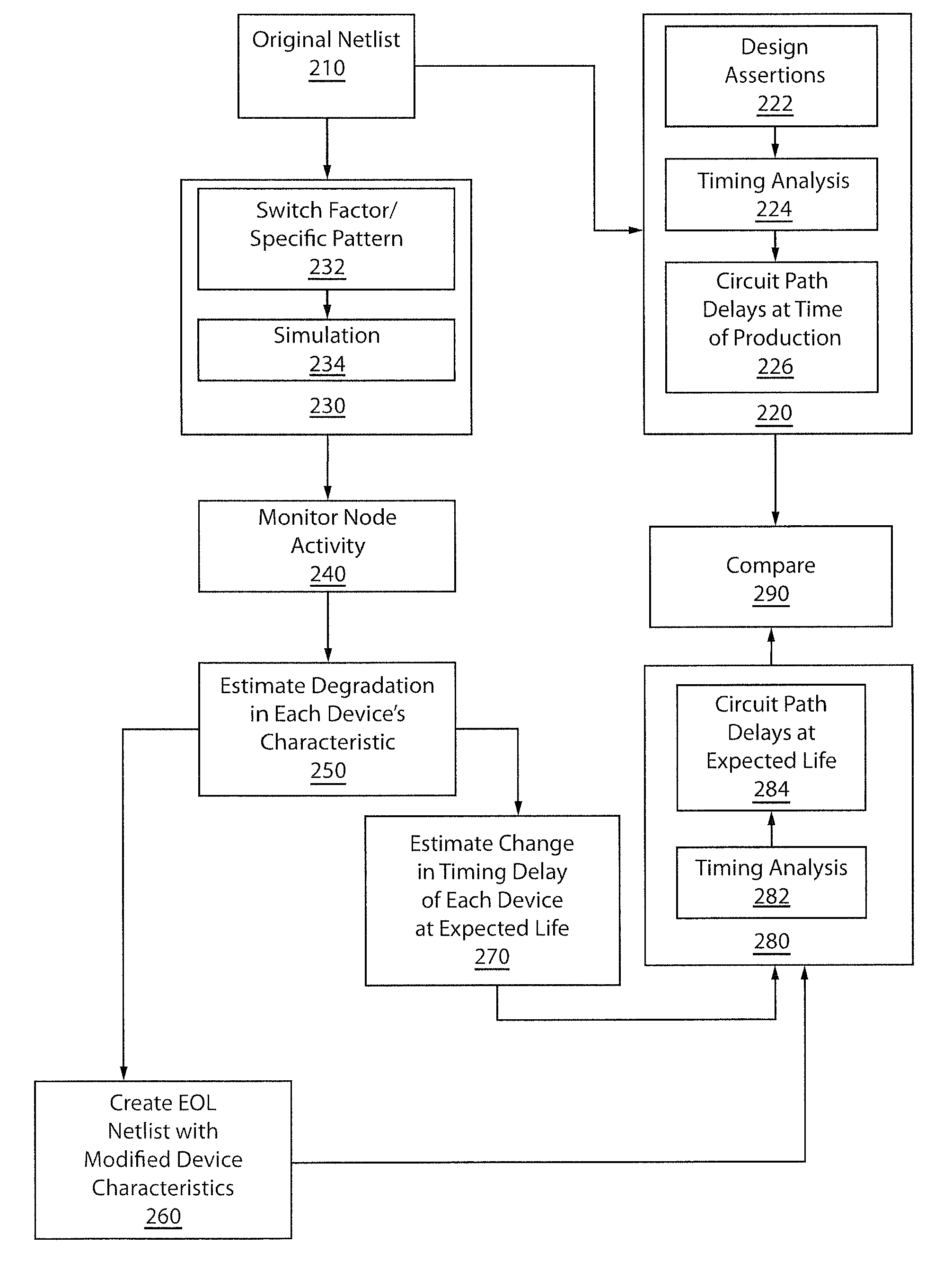
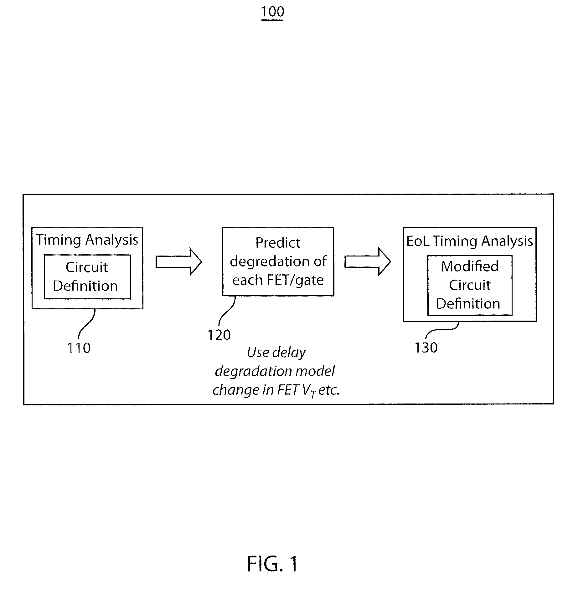
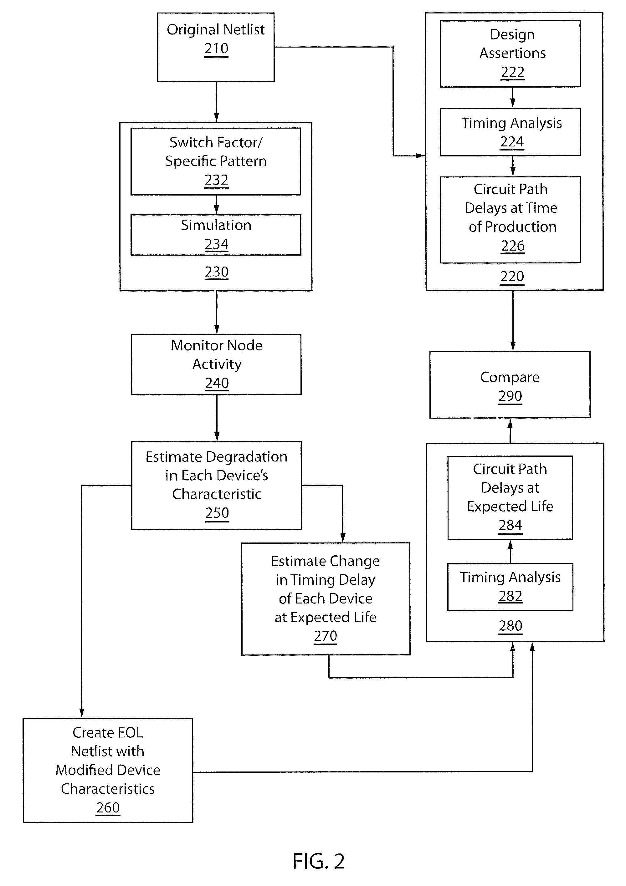
[0020]According to the embodiments of the present principles, a method and system are provided for estimating the extent of degradation in a device at different lifetimes and translating that estimate into a change in circuit performance and shipping frequency. The methods include exercising a circuit using either a specific pattern or a random pattern representative of a workload to be seen by the circuit, performing a simulation to estimate circuit activity and evaluating the possible degradation in the various devices within the circuit at different lifetimes. As a further feature of the embodiments of the present principles, the method provides for utilizing static and statistical timing analysis to evaluate circuit path delays resulting from degradation.

[0021]As will be appreciated by one skilled in the art, aspects of the present invention may be embodied as a system, method or computer program product. Accordingly, aspects of the present invention may take the form of an enti...


PUM


Abstract

A method for estimating delay deterioration in an integrated circuit comprising estimating degradation in at least one characteristic of each device defined within the integrated circuit using voltages and logic values monitored during a simulation of the digital circuit. Generating an end-of-life netlist in which the at least one device characteristic of each device has been modified to reflect the estimated degradation or estimating a change in timing delay of each device directly from the estimated degradation of the at least one characteristic of each device. A timing analysis is performed using the estimated change in timing delay of each device to determine circuit path delays. The timing analysis is static or statistical.

Description

RELATED APPLICATION DATA[0001]This application is a Continuation application of co-pending U.S. patent application Ser. No. 13 / 428,571 filed on Mar. 23, 2012, incorporated herein by reference in its entirety.BACKGROUND[0002]1. Technical Field[0003]The present invention relates to the reliability of integrated circuits, and more particularly to a method for estimating delay deterioration in integrated circuits due to device degradation.[0004]2. Description of the Related Art[0005]Very large scale integration (VLSI) circuits are designed and manufactured using imperfect processes and numerous tests must be run to check the functionality of a VLSI circuit. Such circuits degrade with use over time due to known and predictable effects such as bias temperature instability (BTI) and hot carrier injection (HCI). As a result, manufactured VLSI circuits are more likely to fail in the field, even though they have successfully passed numerous functional and verification tests prior to shipping....

Claims


Application Information

Patent Timeline
Patent Type & Authority Applications(United States)
IPC IPC(8): G06F17/50
CPCG01R31/2881G01R31/31725G01R31/3016G06F30/3312G06F30/39G06F2111/08G06F30/3315G06F2119/12
Inventor BANSAL, ADITYAKIM, JAE-JOONRAO, RAHUL M.
Owner GLOBALFOUNDRIES INC
Features
  • R&D
  • Intellectual Property
  • Life Sciences
  • Materials
  • Tech Scout
  • Unparalleled Data Quality
  • Higher Quality Content
  • 60% Fewer Hallucinations
Learn More