Capacitive touch sensor laminate for display panel device
a touch sensor and display panel technology, applied in the direction of electrical apparatus construction details, instruments, electrical apparatus casings/cabinets/drawers, etc., can solve problems such as display quality deterioration, and achieve the effect of reducing display quality deterioration, preventing warping deformation, and convenient handling
- Summary
- Abstract
- Description
- Claims
- Application Information
AI Technical Summary
Benefits of technology
Problems solved by technology
Method used
Image
Examples
##ventive example 1
Inventive Example 1
[0102](Formation of Undercoat Layer)
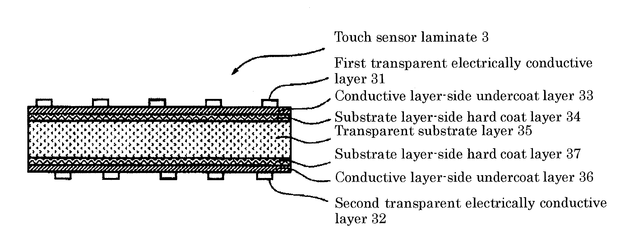
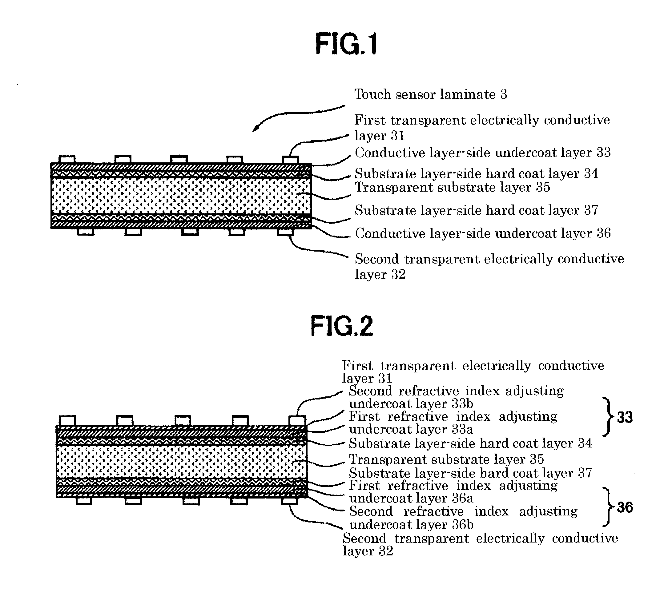
[0103]A thermosetting resin composition containing a melamine resin, an alkyd resin and an organic silane condensate at a weight ratio of 2:2:1 was applied to one surface of a transparent film substrate (refractive index n1=1.65) composed of a 25 μm-thick polyethylene terephthalate film (hereinafter referred to as “PET film”), and then dried and hardened to form a first undercoat layer composed of a 20 nm-thick dielectric layer. In Inventive Example 1, the first undercoat layer had a refractive index n21 of 1.54.
[0104]Then, a second dielectric layer composed of a 10 nm-thick dielectric layer was formed by: diluting silica sol (Colcoat P produced by Colcoat Co., Ltd.) with ethanol to allow a concentration of solid content to become 2 weight %; applying the diluted silica sol to the first undercoat layer by a silica coating method; and drying and hardening the silica sol. The second dielectric layer had a refractive index n22 of 1...
##ventive example 2
Inventive Example 2
[0111]A first undercoat layer composed of a dielectric layer, a second undercoat layer composed of a dielectric layer, and an ITO film were formed on one surface of a PET film to obtain a touch sensor laminate, in the same manner as that in Inventive Example 1.
[0112](Patterning of ITO Film)
[0113]A photoresist patterned in stripes was applied to the transparent conductive layer of the touch sensor laminate, and then dried and hardened. Then, the ITO film was etched by immersing it in a 5 weight % hydrochloric acid solution at 25° C. for 1 minute.
[0114](Patterning of Second Undercoat Layer)
[0115]After etching the ITO film, the second undercoat layer composed of a dielectric film was subsequently etched by immersing it in a 2 weight % sodium hydroxide aqueous solution at 45° C. for 3 minutes, while leaving the laminated photoresist. After completion of the etching, the photoresist was removed.
[0116](Crystallization of ITO Film)
[0117]After patterning the ITO film and ...
##ventive examples 3 and 4
Inventive Examples 3 and 4
[0118]In Inventive Examples 3 and 4, two types of touch sensor laminates each having a pattern area and a pattern opening were prepared in the same manner as those in Inventive Examples 1 and 2. However, Inventive Examples 3 and 4 were different from Inventive Examples 1 and 2, in that the thickness of the first undercoat layer composed of a dielectric layer was set to 35 nm, and the thickness of the second undercoat layer composed of a dielectric layer was set to 5 nm
PUM
 Abstract
Description
Claims
Application Information


