
Method and apparatus for electroplating semiconductor wafer when controlling cations in electrolyte

a technology of electrolyte and electrolyte, which is applied in the direction of coatings, electrolysis components, electrolysis processes, etc., can solve the problems of increasing the defect count, slow/no fill rate of patterned features, and reducing fill rates, so as to reduce the generation of chemical waste, reduce the degradation of organic additives, and improve the stability/longevity of plating solutions

Active Publication Date: 2013-10-31
NOVELLUS SYSTEMS
View PDF9 Cites 19 Cited by
  • Summary
  • Abstract
  • Description
  • Claims
  • Application Information

AI Technical Summary

Benefits of technology

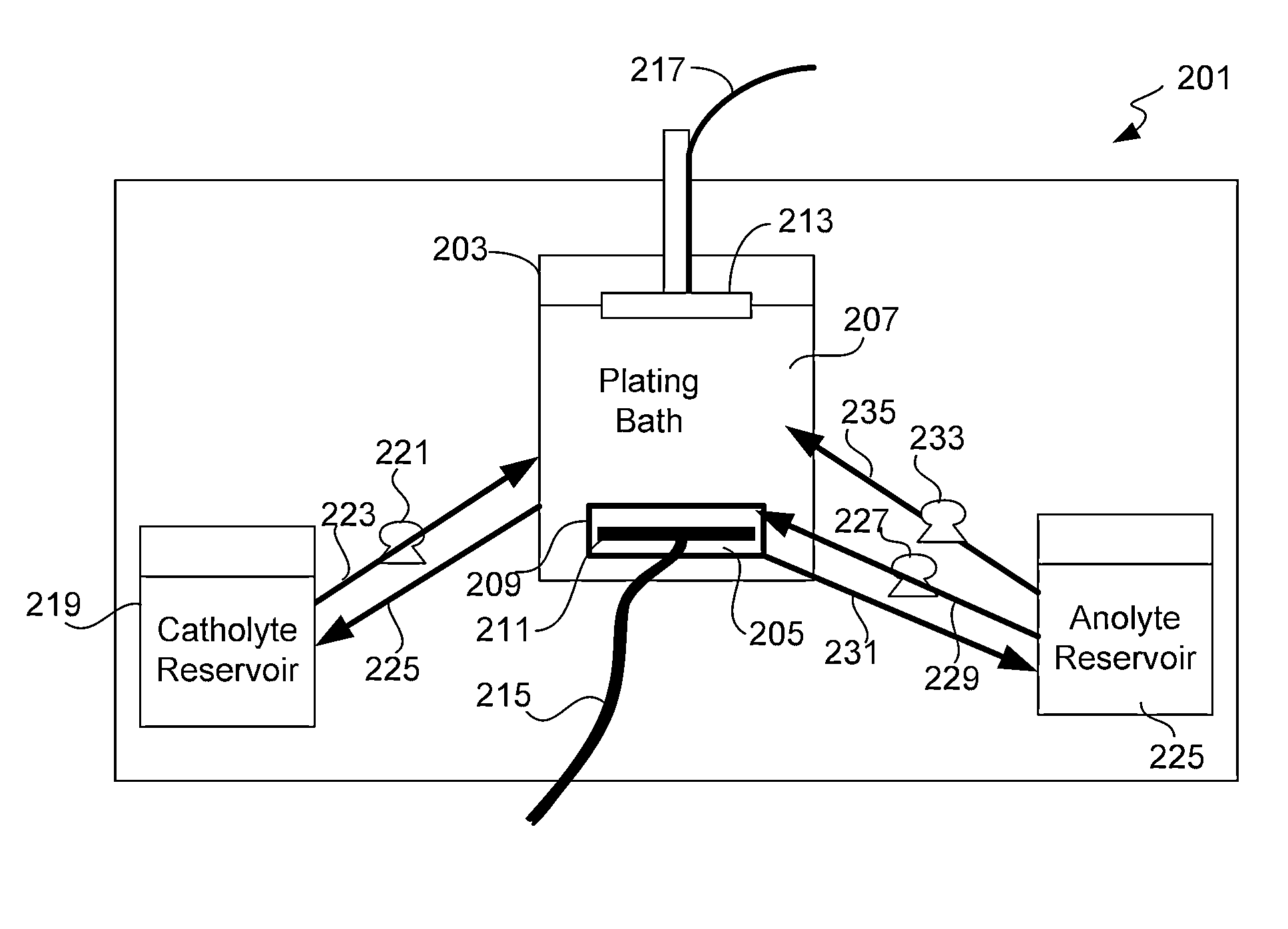
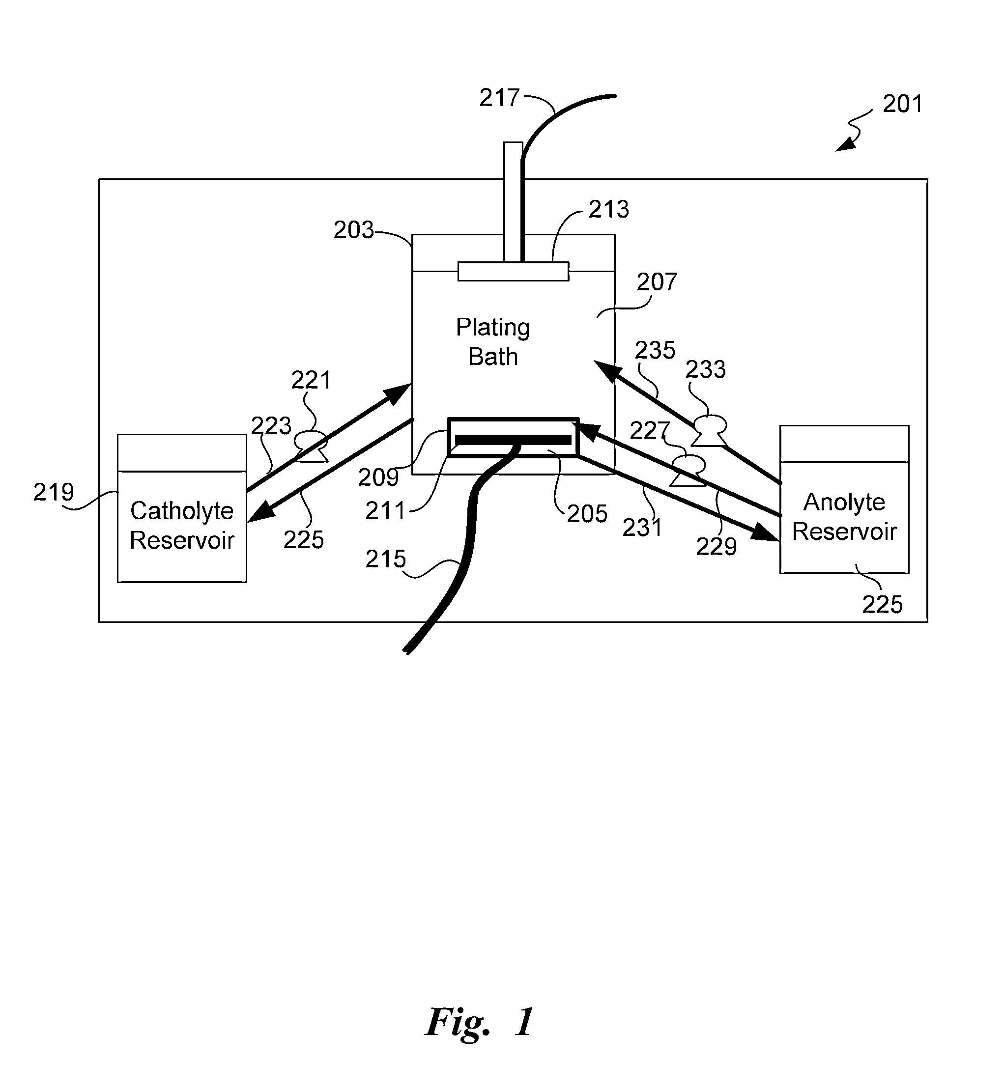
This patent describes an electroplating apparatus that uses a separated anode-cathode chamber to reduce chemical waste and improve plating efficiency. One innovation is controlling the concentrations of cuprous ion (Cu(I)) and oxygen in the solution to prevent the buildup of reactive copper species that can impact plating solution performance. Another innovation is using an impressed current cathodic protection anode (ICCP anode) to counteract a corrosion reaction that produces Cu(I) and maintain a high dissolved oxygen concentration in the solution. Overall, this patent provides technical solutions for improving copper electroplating processes.

Problems solved by technology

Buildup of these complexes in a plating solution can lead to a slow / no fill rate in patterned features on a wafer substrate due to rapid depolarization of the plating solution-substrate interface, voids in features resulting from fill not occurring in a bottom-up fill mechanism, and / or increased defect counts associated with localized rapid nucleation of copper.
Accumulation of these byproducts in a plating solution can result in reduced fill rates, increased defect counts, and increased waste generation.
In addition, breakdown of the accelerator molecules creates an added cost in electroplating processes as the organic additives may need to be more frequently replaced.
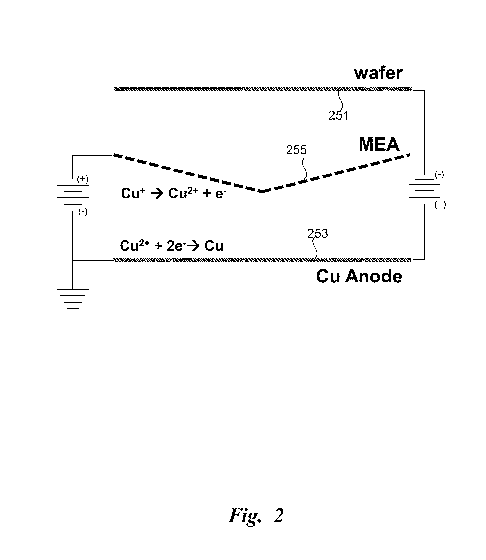
5. The accumulation of Cu(I) itself in the plating solution can lead to changes in plating overpotential and current density, which could alter fill rate and plating performance.
Further, in these embodiments, the ICCP anode may increase the lifespan on the copper anode because it would corrode more slowly and may make the copper concentration in the anolyte and the catholyte more controllable.
Typical membranes used in such devices allow the flow of molecular gasses but do not permit the flow of liquids or solutions which cannot wet the membrane.
With higher temperatures, more oxygen needs to be dissolved into the anolyte due to the reaction kinetics of the copper corrosion at the anode, which may consume dissolved oxygen in the anolyte more rapidly.
The large negative slope values are taken from the rate of depolarization (or suppression loss) of a chronoamperometry experiment and correlate with poor TSV fill performance.

Method used


Image

  • Method and apparatus for electroplating semiconductor wafer when controlling cations in electrolyte
  • Method and apparatus for electroplating semiconductor wafer when controlling cations in electrolyte
  • Method and apparatus for electroplating semiconductor wafer when controlling cations in electrolyte

Examples


Embodiment Construction

[0046]In the following detailed description, numerous specific implementations are set forth in order to provide a thorough understanding of the disclosed implementations. However, as will be apparent to those of ordinary skill in the art, the disclosed implementations may be practiced without these specific details or by using alternate elements or processes. In other instances well-known processes, procedures, and components have not been described in detail so as not to unnecessarily obscure aspects of the disclosed implementations.

[0047]In this application, the terms “semiconductor wafer,”“wafer,”“substrate,”“wafer substrate,” and “partially fabricated integrated circuit” are used interchangeably. One of ordinary skill in the art would understand that the term “partially fabricated integrated circuit” can refer to a silicon wafer during any of many stages of integrated circuit fabrication thereon. The following detailed description assumes the disclosed implementations are imple...


PUM

PropertyMeasurementUnit
thicknessaaaaaaaaaa
temperatureaaaaaaaaaa

Abstract

Apparatus and methods for electroplating metal onto substrates are disclosed. The electroplating apparatus comprise an electroplating cell and at least one oxidization device. The electroplating cell comprises a cathode chamber and an anode chamber separated by a porous barrier that allows metal cations to pass through but prevents organic particles from crossing. The oxidation device (ODD) is configured to oxidize cations of the metal to be electroplated onto the substrate, which cations are present in the anolyte during electroplating. In some embodiments, the ODD is implemented as a carbon anode that removes Cu(I) from the anolyte electrochemically. In other embodiments, the ODD is implemented as an oxygenation device (OGD) or an impressed current cathodic protection anode (ICCP anode), both of which increase oxygen concentration in anolyte solutions. Methods for efficient electroplating are also disclosed.

Description

CROSS-REFERENCE TO RELATED APPLICATIONS[0001]The present application claims the benefit of and priority to U.S. Provisional Patent Application No. 61 / 639,783, entitled “Apparatus for Oxygenation of Separated Anode Chambers,” filed Apr. 27, 2012, and U.S. Provisional Patent Application No. 61 / 666,390, entitled “Electroplating Apparatus Including Auxiliary Electrodes,” filed Jun. 29, 2012, which applications are fully incorporated herein by reference in their entirety.BACKGROUND[0002]1. Field of the Invention[0003]This invention generally relates to electroplating metal layers onto substrates. More specifically, it relates to apparatus for controlling the composition, flow, and potential distribution of electrolyte while electroplating a wafer.[0004]2. Related Technology[0005]In electronics, a wafer (also called a slice or substrate) is a thin slice of semiconductor material, such as a silicon crystal, used in the fabrication of integrated circuits and other microdevices. The wafer se...

Claims


Application Information

Patent Timeline
Patent Type & Authority Applications(United States)
IPC IPC(8): C25D21/14C25D17/00C25D3/38
CPCC25D21/14C25D3/38C25D17/001C25D17/002C25D21/12C25D21/18C25D5/18C25D7/12
Inventor SPURLIN, TIGHE A.MERRILL, CHARLES L.HUANG, LUDANTHORUM, MATTHEWBROGAN, LEEDUNCAN, JAMES E.WILMOT, FREDERICK D.STOWELL, MARSHALL R.MAYER, STEVEN T.FU, HAIYINGPORTER, DAVID W.GHONGADI, SHANTINATHREID, JONATHAN D.LEE, HYOSANG S.WILLEY, MARK J.
Owner NOVELLUS SYSTEMS
Learn More